
Bilayer metal capping layer for interconnect applications

Inactive Publication Date: 2009-09-03
IBM CORP
View PDF20 Cites 24 Cited by
  • Summary
  • Abstract
  • Description
  • Claims
  • Application Information

AI Technical Summary

Benefits of technology

[0012]The present invention provides semiconductor interconnect structures that have improved reliability and technology extendibility. In the present invention, a second metallic capping layer is selectively located on a surface of a first metallic cap layer which is, in turn, selectively located on a surface of the conductive feature embedded within a first dielectric material. Both the first and second metallic capping layers are located beneath an opening, e.g., a via opening, that is present within an overlying second dielectric material. The second metallic capping layer protects the first metallic capping layer from being removed (either completely or partially) during subsequent processing steps. Interconnect structures including via gouging features as well as non-via gouging features are disclosed. The present invention provides methods of fabricating such semiconductor interconnect structures which are compatible with existing semiconductor interconnect processing steps.
[0016]In addition to providing semiconductor structures, the present invention also provides methods of forming the same. The inventive methods include processing steps that are compatible with current interconnect processing steps, as such, the inventive methods can be easily integrated into existing interconnect processing.

Problems solved by technology

EM is one of the worst reliability concerns for very large scale integrated (VLSI) circuits.
The EM initial voids first nucleate at the metal / dielectric cap interface and then grow in the direction of the bottom of the interconnect, which eventually results in a circuit dead opening.
For example, CoWP metallic capping layers may be damaged or removed (partially or completely) by a subsequent etching step using dilute hydrofluoric acid (DHF) as a chemical etchant.
The attack or removal (partial or complete) of the metallic capping layer in an interconnect structure is undesirable in that it leads to increased EM within the interconnect structure.

Method used


Image

  • Bilayer metal capping layer for interconnect applications
  • Bilayer metal capping layer for interconnect applications
  • Bilayer metal capping layer for interconnect applications

Examples


Embodiment Construction

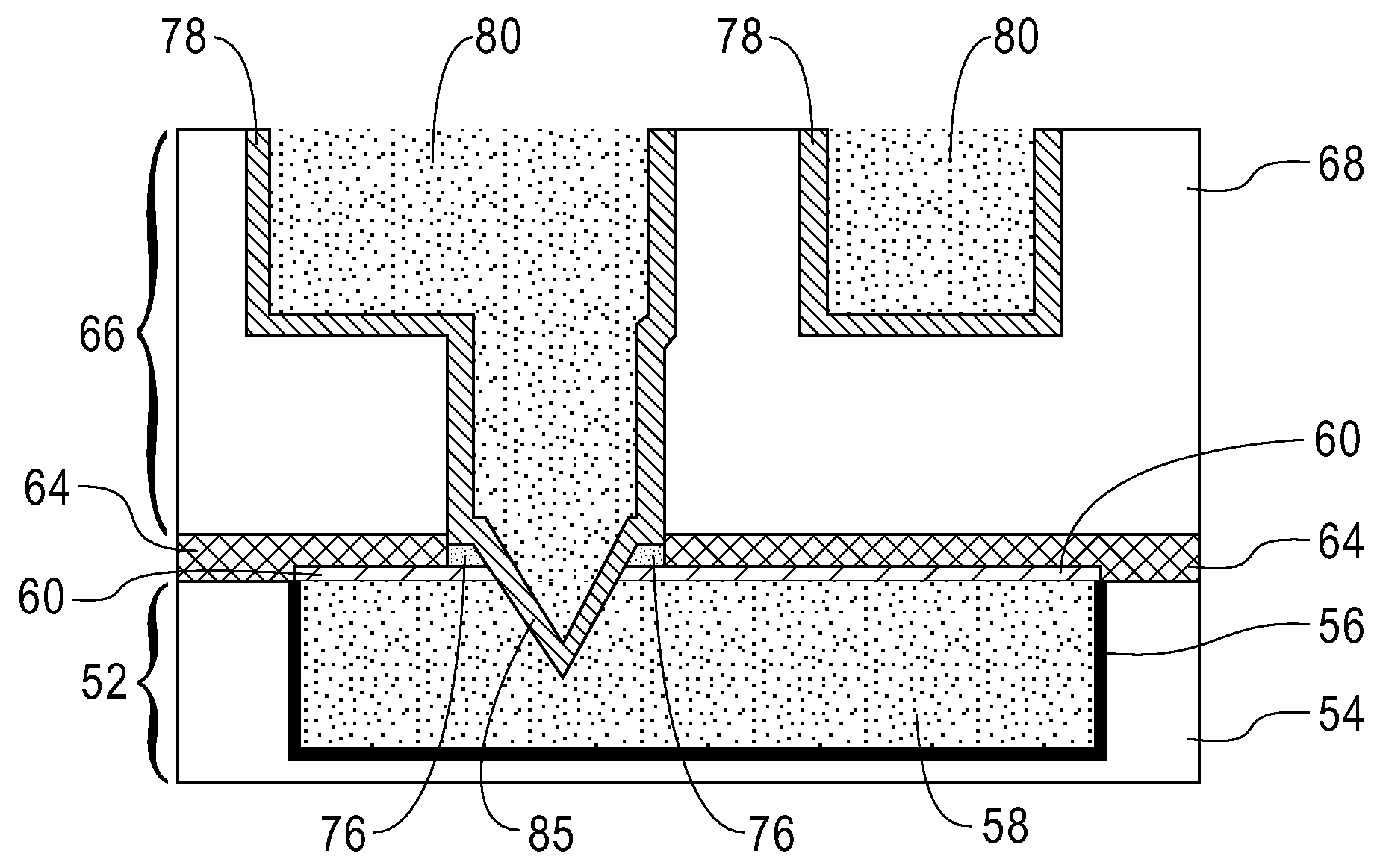
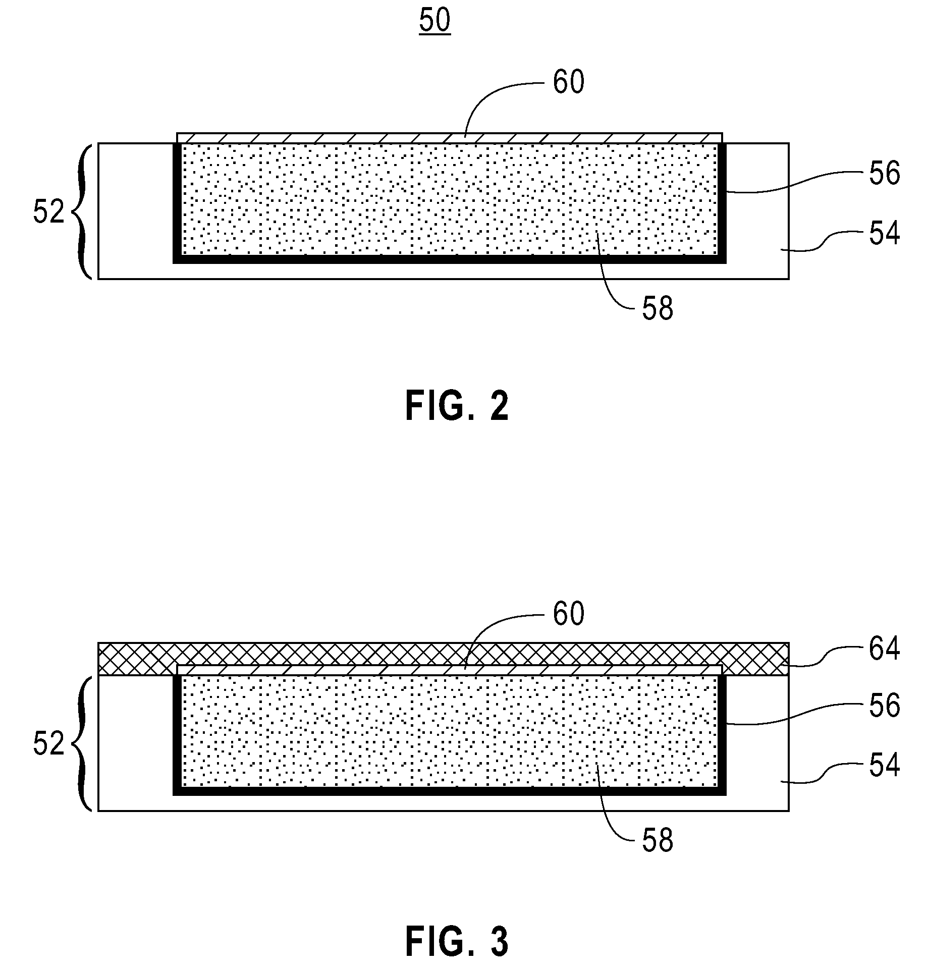
[0022]The present invention, which provides interconnect structures having technology extendibility and high reliability and methods of fabricating the same, will now be described in greater detail by referring to the following discussion and drawings that accompany the present application. It is noted that the drawings of the present application are provided for illustrative purposes only and, as such, the drawings are not drawn to scale.

[0023]In the following description, numerous specific details are set forth, such as particular structures, components, materials, dimensions, processing steps and techniques, in order to provide a thorough understanding of the present invention. However, it will be appreciated by one of ordinary skill in the art that the invention may be practiced without these specific details. In other instances, well-known structures or processing steps have not been described in detail in order to avoid obscuring the invention.

[0024]It will be understood that ...


PUM


Abstract

The invention provides semiconductor interconnect structures that have improved reliability and technology extendibility. In the present invention, a second metallic capping layer is located on a surface of a first metallic cap layer which is, in turn, located on a surface of the conductive feature embedded within a first dielectric material. Both the first and second metallic capping layers are located beneath an opening, e.g., a via opening, the is present within an overlying second dielectric material. The second metallic capping layer protects the first dielectric capping layer from being removed (either completely or partially) during subsequent processing steps. Interconnect structures including via gouging features as well as non-via gouging features are disclosed. The present invention provides methods of fabricating such semiconductor interconnect structures.

Description

FIELD OF THE INVENTION[0001]The present invention relates to a semiconductor interconnect structure and a method of fabricating the same. More particularly, the present invention relates to a semiconductor interconnect structure in which a bilayer metal capping layer is present within the interconnect structure. The present invention also provides a method of fabricating a semiconductor interconnect structure including a bilayer metal capping layer.BACKGROUND OF THE INVENTION[0002]Generally, semiconductor devices include a plurality of circuits which form an integrated circuit (IC) fabricated on a semiconductor substrate. A complex network of signal paths will normally be routed to connect the circuit elements distributed on the surface of the substrate. Efficient routing of these signals across the device requires formation of multilevel or multilayered schemes, such as, for example, single or dual damascene wiring structures. The wiring structure typically includes copper, Cu, sin...

Claims


Application Information

Patent Timeline
IPC IPC(8): H01L21/768H01L23/538
CPCH01L21/76805H01L21/76814H01L21/76843H01L21/76846H01L21/76849H01L2924/0002H01L23/5226H01L23/53238H01L2924/00
Inventor YANG, CHIH-CHAONITTA, SATYA V.
Owner IBM CORP
Learn More