Probe card

a technology of a probe card and a chip body, which is applied in the field of probe cards, can solve the problems of increasing the number of dies and increasing the cost, and achieve the effect of economic low-cost and excellent transmission characteristics

Active Publication Date: 2009-09-03
NHK SPRING CO LTD
View PDF8 Cites 30 Cited by
  • Summary
  • Abstract
  • Description
  • Claims
  • Application Information

AI Technical Summary

Benefits of technology

[0016]According to the present invention, it is possible to provide an economical low-cost probe card excellent in transmission characteristics of high-frequency electrical signals by providing a plurality of probes that contact a plurality of electrodes formed on a semiconductor wafer which is a test object to input or output electrical signals to or from the electrodes, a probe head that holds the probes, a substrate...

Problems solved by technology

However, because hundreds to tens of thousands of dies are present on one semiconductor wafer, it takes conside...

Method used


Image

  • Probe card
  • Probe card
  • Probe card

Examples


first embodiment

Modification of First Embodiment

[0102]FIG. 4 is a plan view of a structure of a probe card according to a modification of the first embodiment. A probe card 11 shown in this figure has a reinforcing element 9 attached to a substrate 4-2 structured in the same manner as the substrate 4. The reinforcing element 9 includes a circular outer peripheral portion 91 fitted around the outer periphery of the substrate 4-2, spokes 92 that extend from the inner side face of the outer peripheral portion 91 toward the center of the circle formed by the outer peripheral portion 91, and a central portion 93 formed in a disc shape having a center the same as that of the circle of the outer peripheral portion 91 and connected to the outer peripheral portion 91 via the spokes 92.

[0103]When the reinforcing element 9 is to be attached, the reinforcing element 9 is attached to the substrate 4-2 from its connection side to the test equipment (rear side of FIG. 1) and the spokes 92 and the central portion ...

second embodiment

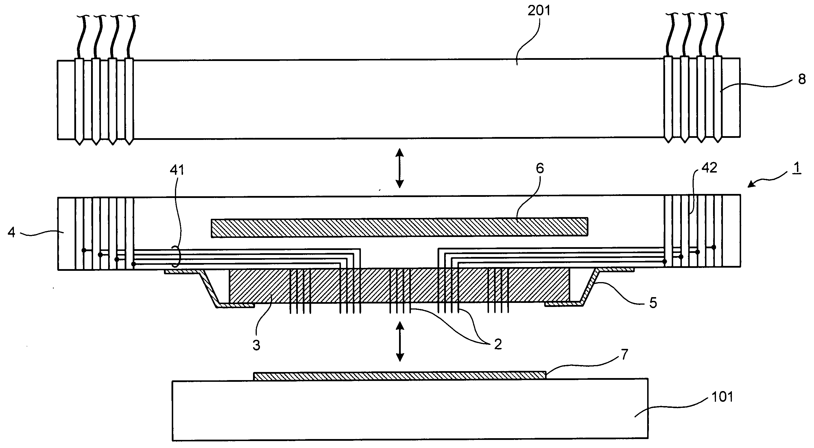
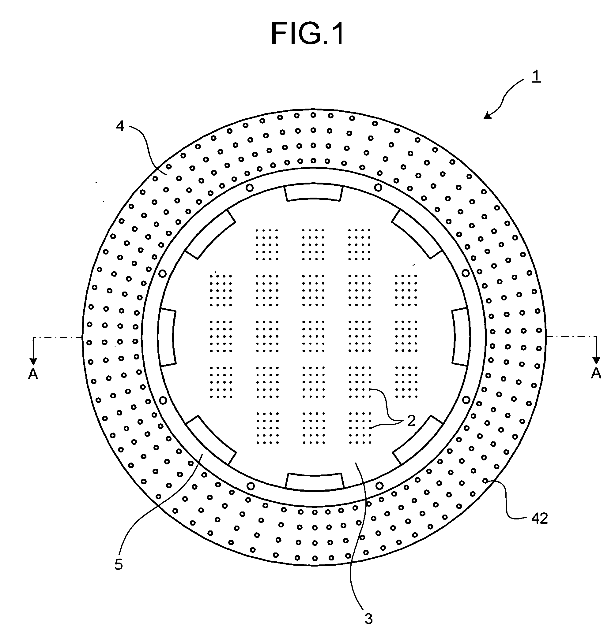
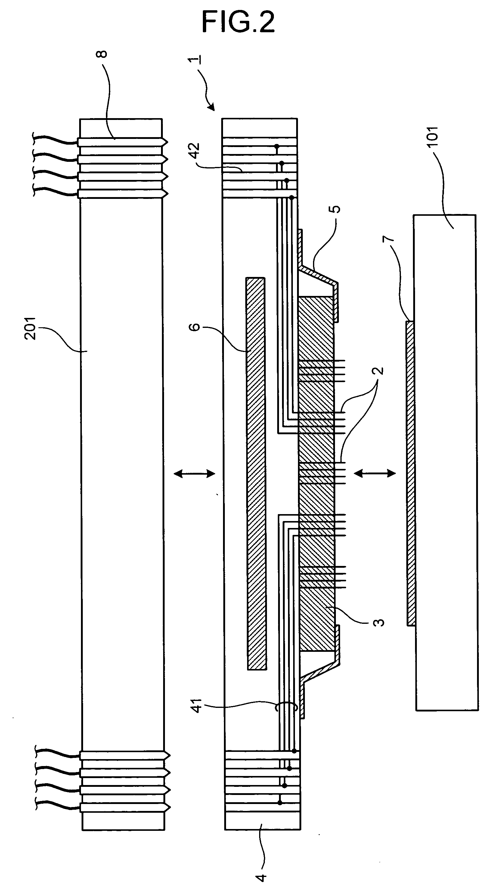
[0105]FIG. 5 is a plan view of a structure of a probe card according to a second embodiment of the present invention. FIG. 6 is a cross section of part of a cross-sectional structure taken along the line B-B of FIG. 5. A probe card 12 as shown in these figures includes the probes 2 arranged according to a test object, the disc-like probe head 3 that holds the probes 2, a disc-like substrate 13 having its diameter larger than that of the probe head 3, the holding element 5 fixed to the substrate 13 and formed of a disc spring or a plate spring or the like to hold the probe head 3, a core layer 14 formed of a material which is layered and buried in the substrate 13 so as to have the same surface area as that of the substrate 13, and has a coefficient of thermal expansion lower than that of the substrate 13, and a plurality of male connectors 15 radially arranged with respect to the center of the substrate 13 so as to be connected to the test equipment.

[0106]The male connector 15 is pa...

third embodiment

[0116]FIG. 9 is a plan view of a structure of a probe card according to a third embodiment of the present invention. FIG. 10 is a cross section of part of a cross-sectional structure taken along the line D-D of FIG. 9. A probe card 17 shown in these figures includes the probes 2 arranged corresponding to a test object, the disc-like probe head 3 that holds the probes 2, a disc-like substrate 18 having its diameter larger than that of the probe head 3, the holding element 5 fixed to the substrate 18 and formed of a disc spring or a plate spring or the like to hold the probe head 3, a core layer 20 formed of a material which is layered and buried in the substrate 18 so as to have a surface area the same size as the surface area of the substrate 18, and which has a coefficient of thermal expansion lower than that of the substrate 18, and a plurality of ZIF type male connectors 19 radially arranged with respect to the center of the substrate 18 so as to be connected to the test equipmen...


PUM


Abstract

A probe card includes a plurality of probes that contacts a plurality of electrodes provided in the semiconductor wafer and that inputs or outputs an electrical signal in or from the electrodes, a probe head that holds the probes, a substrate having a wiring which is provided near the surface of the substrate facing the probe head so as to be contactable with the probe head and is connected to the probes, a core layer formed of a material which is buried in the substrate and has a coefficient of thermal expansion lower than that of the substrate, and a connecting member that electrically connects at least some of the probes with an external device via the wiring.

Description

TECHNICAL FIELD[0001]The present invention relates to a probe card that inputs or outputs an electrical signal to or from a plurality of areas of a semiconductor wafer which is a test object.BACKGROUND ART[0002]In the process of testing a semiconductor, electrical continuity of the semiconductor in a state of a semiconductor wafer before being diced is tested by contacting a conductive probe with the semiconductor wafer and a defective piece is sometimes detected (WLT: Wafer Level Test). When conducting the WLT, a probe card that contains many probes is used to deliver test signals from test equipment (tester) to the semiconductor wafer. Generally, in the WLT, each probe is made to contact each die when scanning the die on the semiconductor wafer with the probe card. However, because hundreds to tens of thousands of dies are present on one semiconductor wafer, it takes considerably long time for testing one semiconductor wafer, and an increase in the number of dies causes an increas...

Claims


Application Information

Patent Timeline
IPC IPC(8): G01R31/02G01R1/067
CPCG01R1/44G01R1/07314H01L22/00G01R1/073
Inventor SASAKI, SHUNSUKENAKAYAMA, HIROSHI
Owner NHK SPRING CO LTD
Why Eureka
Try Eureka