Imaging apparatus and image signal processing method

a technology of image signal processing and image apparatus, which is applied in the field of image signal processing method and image apparatus, can solve problems such as image capture failure, and achieve the effect of wide dynamic range and reduced probability of failed image captur

Active Publication Date: 2009-09-03
FUJIFILM CORP
View PDF5 Cites 24 Cited by
  • Summary
  • Abstract
  • Description
  • Claims
  • Application Information

AI Technical Summary

Benefits of technology

[0020]According to the invention, the probability of failed image capturing can be reduced an

Problems solved by technology

In JP 2007-256907 A, there is a time difference between the two kinds of shooting, so that there is a problem that image capturing may be failed because facial expression will bec

Method used


Image

  • Imaging apparatus and image signal processing method
  • Imaging apparatus and image signal processing method
  • Imaging apparatus and image signal processing method

Examples


first embodiment

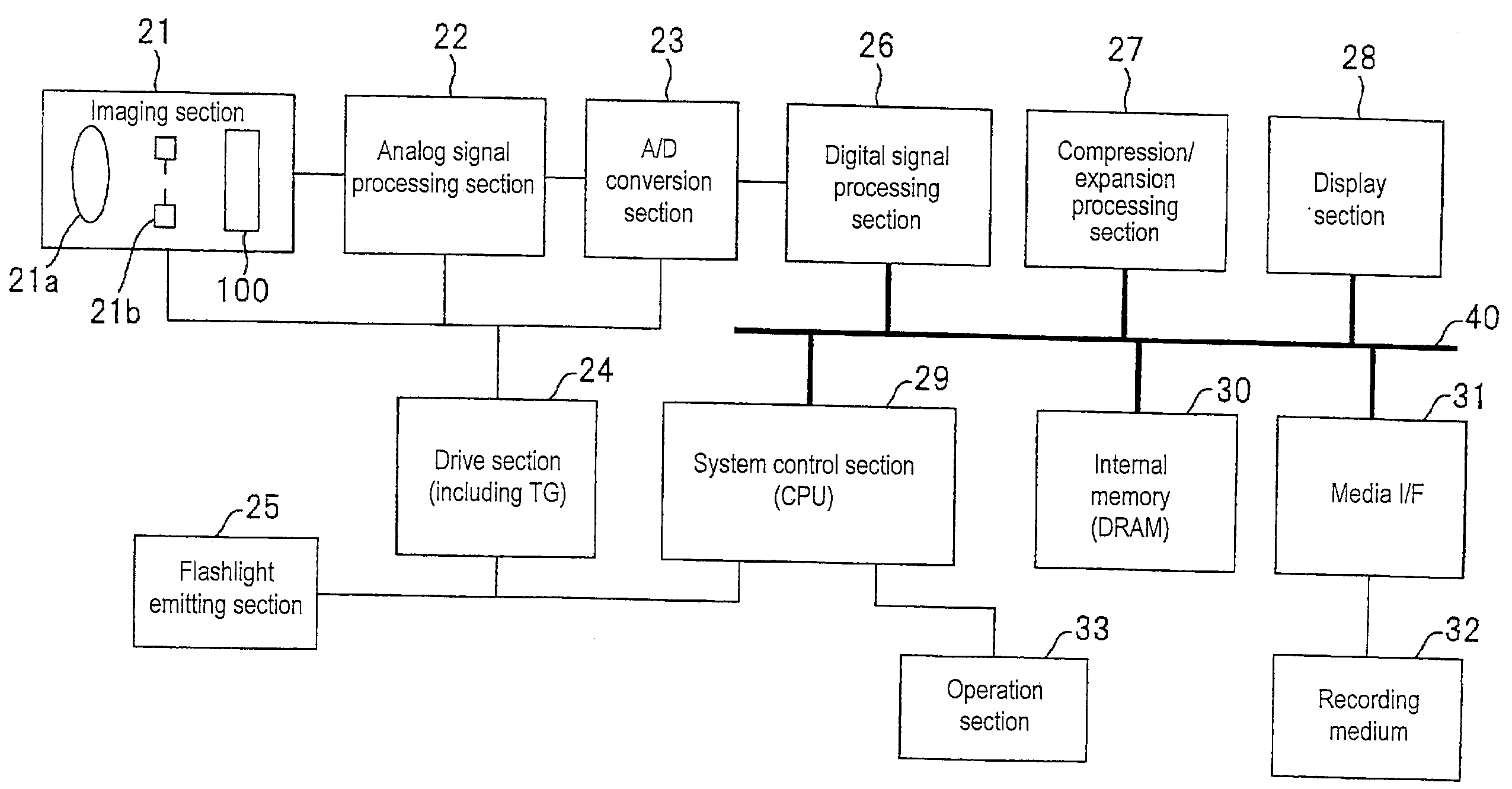
[0033]FIG. 1 is a functional block diagram showing the configuration of a digital camera according to the invention. This digital camera includes an imaging section 21, an analog signal processing section 22, an analog-to-digital (A / D) conversion section 23, a drive section (including a timing generator TG) 24, and a flashlight emitting section 25. The analog signal processing section 22 performs analog processing such as auto gain control (AGC), correlated double sampling, etc. for analog image data output from the imaging section 21. The A / D conversion section 23 converts the analog image data output from the analog signal processing section 22 into digital image data. The drive section 24 performs drive control of the A / D conversion section 23, the analog signal processing section 22 and the imaging section 21 in accordance with an instruction issued from a system control section (CPU) 29 which will be described later. The flashlight emitting section 25 emits flashlight in accord...

second embodiment

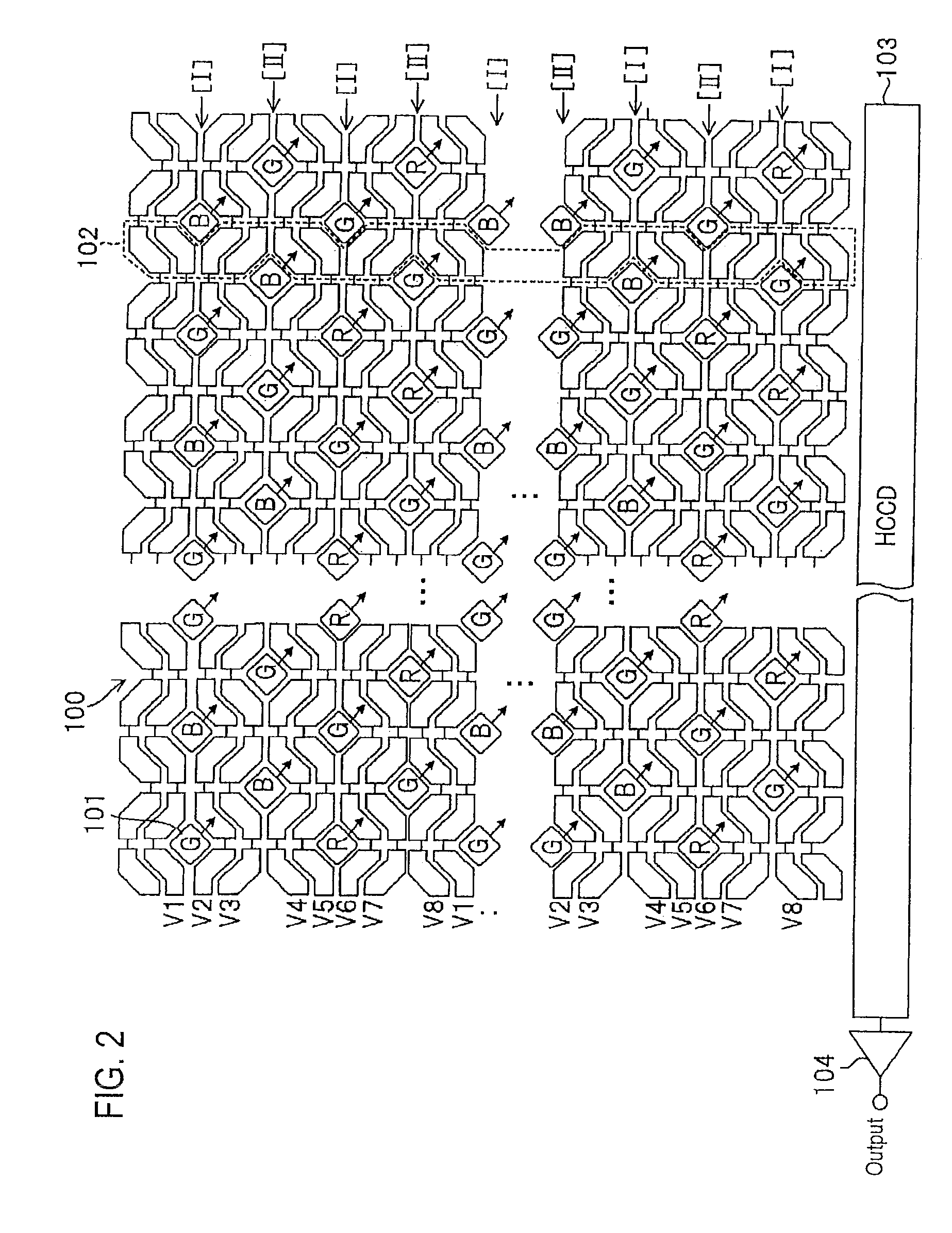
[0079]FIG. 10 is a schematic view of a surface of a solid-state imaging device 200 having pixels arranged as a tetragonal lattice array according to the invention. The solid-state imaging device 200 has pixels 201 arranged as a tetragonal lattice array, vertical charge transfer paths 202 formed along respective columns of the pixels, a horizontal charge transfer path 203 formed along respective end portions of the vertical charge transfer paths 202 in the transfer direction, and an output amplifier 204 provided in an output end portion of the horizontal change transfer path 203.

[0080]Two transfer electrodes per pixel are provided to form the vertical charge transfer paths. Reading gates 205 are provided in even-numbered transfer electrodes V2, V4, V6 and V8.

[0081]In the illustrated example, color filters are arranged so that two rows each having an arrangement “BGRGBGRG . . . ” and two rows each having an arrangement “RGBGRGBG . . . ” are alternated vertically every two rows. A grou...

third embodiment

[0083]FIG. 11 is a schematic view of a surface of a solid-state imaging device 300 having pixels arranged as a tetragonal lattice array according to the invention. The solid-state imaging device 300 has the same color filter arrangement as that of the solid-state imaging device 200 shown in FIG. 10.

[0084]Difference of the solid-state imaging device 300 from the solid-state imaging device 200 is as follows. Read gates 305 for reading signal charge from respective pixels 301 to vertical charge transfer paths 302 are provided in transfer electrodes (vertically upper and lower transfer electrodes) which vary between pixels horizontally and vertically adjacent to each other. Consequently, among the pixels arranged as a tetragonal lattice array, pixels located in one checkered pattern form a first pixel group (or a second pixel group) while the remaining pixels located in the other checkered pattern form a second pixel group (or a first pixel group).

[0085]The solid-state imaging device 30...


PUM


Abstract

An imaging apparatus includes an imaging device, an imaging device deriving unit and a signal processing unit. Pixels of the imaging device include a first pixel group and a second pixel group. The imaging device driving unit exposes the first pixel group during a first exposure period, exposes the second pixel group during a second exposure period, and reads first image data captured by the first pixel group and second image data captured by the second pixel group separately. The signal processing unit performs image processing for the first and second image data. A first shooting mode and a second shooting mode are provided. In the first shooting mode, the signal processing unit performs the image processing for the first and second image data separately to generate two pieces of subject image data. In the second shooting mode, the signal processing unit combines the first and second image data.

Description

CROSS-REFERENCE TO RELATED APPLICATIONS[0001]This application is based upon and claims the benefit of priority from the Japanese Patent Application No. 2008-48055 filed on Feb. 28, 2008, the entire contents of which are incorporated herein by reference.BACKGROUND OF THE INVENTION[0002]1. Technical Field[0003]The invention relates to an imaging apparatus equipped with a solid-state imaging device and an image signal processing method used in the imaging apparatus. Particularly, the invention relates to an imaging apparatus that can capture an image of a subject with a wide dynamic range and that can capture continuous two images (e.g. a flashed image and a non-flashed image) in one shooting operation, and an image signal processing method used in the imaging apparatus.[0004]2. Related Art[0005]A solid-state imaging device such as a CCD image sensor or a CMOS image sensor having at least millions of pixels mounted on one chip has become popular recently with the advance of increase in...

Claims


Application Information

Patent Timeline
IPC IPC(8): H04N5/335H04N5/222H04N5/232H04N5/238H04N5/243H04N101/00
CPCH04N5/2353H04N5/2354H04N5/35581H04N5/35554H04N5/2355H04N23/741H04N23/73H04N23/74H04N25/583H04N25/589
Inventor KOBAYASHI, HIROKAZUKUSUDA, DAISUKETAMARU, MASAYACHO, MICHIOODA, KAZUYA
Owner FUJIFILM CORP
Why Eureka
Try Eureka