Semiconductor device and the method of manufacturing the same

a technology of semiconductor devices and mosfets, which is applied in the direction of semiconductor devices, basic electric elements, electrical equipment, etc., can solve the problems of high breakdown voltage of power mosfets, and achieve the reduction of on-state resistance, high breakdown voltage, and high breakdown voltage

Inactive Publication Date: 2009-09-10
FUJI ELECTRIC SYST CO LTD
View PDF7 Cites 4 Cited by
  • Summary
  • Abstract
  • Description
  • Claims
  • Application Information

AI Technical Summary

Benefits of technology

[0017]According to a second aspect of the invention, there is provided a method of manufacturing the semiconductor device described above, the method including forming the second drain region by the tilt angle ion implantation of an impurity of the first conductivity type. According to the invention, a thick oxide film is formed locally on the pillar section, which is the section of the semiconductor substrate sandwiched between the trenches. By making the thick oxide film work for a field plate, a high breakdown voltage is obtained. Further, by forming a second n-type drain region on the side wall of a p-type region formed in the pillar section, the p-type region is made to work for a p-type RESURF region that relaxes the electric field.
[0018]Due to the structure described above, a high breakdown voltage is obtained even if the second n-type drain region is doped more heavily. Therefore, by doping the second drift region more heavily, the ON-state resistance is reduced with no problem. In other words, the thick oxide film and the p-type RESURF region facilitate improving the tradeoff relation between the breakdown voltage and the ON-state resistance and obtaining a semiconductor device that exhibits a high breakdown voltage and low ON-state resistance.

Problems solved by technology

Moreover, when an input voltage is high, it is required for the power MOSFETs to exhibit a high breakdown voltage.

Method used


Image

  • Semiconductor device and the method of manufacturing the same
  • Semiconductor device and the method of manufacturing the same
  • Semiconductor device and the method of manufacturing the same

Examples


second embodiment

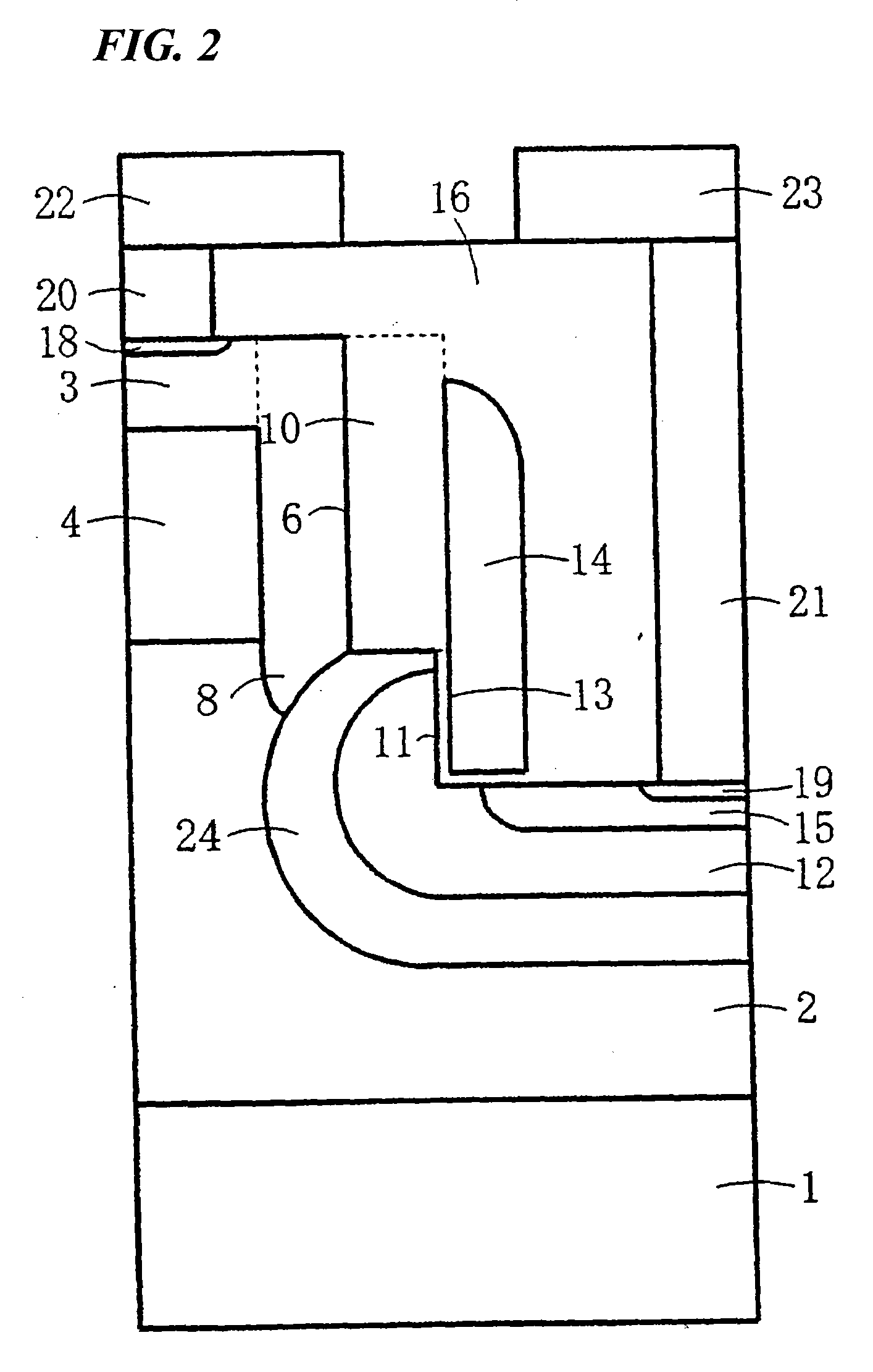
[0041]FIG. 2 is a cross sectional view of a semiconductor device according to the invention. The semiconductor device shown in FIG. 2 is different from the semiconductor device shown in FIG. 1 in the following point. In FIG. 2, n-type body region 24 is formed in the bottom portion of first trench 6 such that n-type body region 24 is surrounding p-type base region 12. The impurity concentration in n-type body region 24 is set to be higher than the impurity concentration in n-type well region 2. This impurity concentration distribution is employed to prevent foreseeable punch-through that may be caused between p-type RESURF region 4 and p-type base region 12 in the structure shown in FIG. 1 from occurring. It is possible for forming an n-type body region (n-type buffer region) in the trench bottom to raise the punch-through breakdown voltage.

third embodiment

[0042]FIG. 3 is a cross sectional view of a semiconductor device according to the invention. The semiconductor device shown in FIG. 3 is different from the semiconductor device shown in FIG. 2 in the following points. First, second trench 11 is not formed in FIG. 3 and the bottom of first trench 6 is positioned as deeply as the bottom of second trench 11 in FIG. 2. Second, gate insulator film 13 is formed between second drain region 8 and gate electrode 14 but thick oxide film 10 is not in FIG. 3. This structure facilitates improving the tradeoff relation between the breakdown voltage and the ON-state resistance. In FIG. 3, n-type body region 24 may not be formed with no problem in the same manner as in FIG. 1.

fourth embodiment

[0043]FIG. 4 is a cross sectional view of a semiconductor device according to the invention. The semiconductor device shown in FIG. 4 is different from the semiconductor device shown in FIG. 1 in the following point. In FIG. 4, first n-type drain region 3 is formed more deeply than in FIG. 1 and p-type RESURF region 4 is formed in first n-type drain region 3. In this structure, the impurity concentration in the portion of first n-type drain region 3 under p-type RESURF region 4, namely the portion of first n-type drain region 3 located between the p-type RESURF region 4 and the n-type well region 2, is close to the impurity concentration in n-type well region 2. Therefore, the semiconductor device shown in FIG. 4 exhibits the effects similar to the effects that the semiconductor device shown in FIG. 1 exhibits.

[0044]In the semiconductor devices according to the second and third embodiments, p-type RESURF region 4 may be formed in first n-type drain region 3 with no problem. The modi...


PUM


Abstract

A power MOSFET exhibits a high breakdown voltage and low ON-state resistance. The device includes a trench formed in a semiconductor substrate, a gate electrode located along a side wall of the trench and a bottom wall of the trench near a side wall thereof, a pillar section, a first drain region of a first conductivity type in the pillar section, a base region of a second conductivity type in contact with the side wall of the trench in a bottom portion thereof and the bottom wall of the trench, a source region of the first conductivity type in a surface portion of the base region, a RESURF region of the second conductivity type in the pillar section, the RESURF region being formed in contact with the first drain region; and a second drain region of the first conductivity type in a side wall surface portion of the pillar section.

Description

BACKGROUND[0001]The present invention relates to power MOSFETs and such semiconductor devices used in power supply ICs, motor driving ICs for driving a motor and such power ICs. It is required for the power MOSFETs and such semiconductor devices to exhibit low ON-state resistance and a high breakdown voltage and to perform high-speed switching. The present invention relates also to the method of manufacturing the power MOSFETs and such semiconductor devices described above.[0002]It is usually required for power MOSFETs incorporated in a power supply IC to exhibit low ON-state resistance and to perform high-speed switching. Moreover, when an input voltage is high, it is required for the power MOSFETs to exhibit a high breakdown voltage. The power MOSFETs, which facilitate obtaining a high breakdown voltage and low ON-state resistance, include a trench lateral power MOSFET (hereinafter referred to as a “TLPM”).[0003]FIG. 13 is a cross sectional view of a conventional TLPM. FIG. 13 sho...

Claims


Application Information

Patent Timeline
Patent Type & Authority Applications(United States)
IPC IPC(8): H01L29/78H01L21/336
CPCH01L21/2815H01L29/063H01L29/0878H01L29/41766H01L29/4236H01L29/7825H01L29/42376H01L29/66689H01L29/66696H01L29/66704H01L29/42368
Inventor KITAMURA, MUTSUMI
Owner FUJI ELECTRIC SYST CO LTD
Why Eureka
Try Eureka