Method of manufacturing wiring substrate and method of manufacturing semiconductor device

a manufacturing method and semiconductor technology, applied in the direction of basic electric elements, layered products, chemistry apparatus and processes, etc., can solve the problems of high cost, increased inductance at the connection portion, and difficulty in achieving sufficient performance and size reduction, etc., to achieve high efficiency and low cost

Active Publication Date: 2009-09-24
SHINKO ELECTRIC IND CO LTD
View PDF5 Cites 55 Cited by
  • Summary
  • Abstract
  • Description
  • Claims
  • Application Information

AI Technical Summary

Benefits of technology

[0016]Exemplary embodiments of the present invention provide a method of manufacturing a wiring substrate and a method of manuf

Problems solved by technology

However, it is difficult to achieve sufficiently a higher performance and a size reduction by this method.
Also, in this structure that the chip component and the pads of the build-up wiring layer are connected electrically via the bumps, such a problem arises that an inductance at the connection portion is increased, in particular, an operati

Method used


Image

  • Method of manufacturing wiring substrate and method of manufacturing semiconductor device
  • Method of manufacturing wiring substrate and method of manufacturing semiconductor device
  • Method of manufacturing wiring substrate and method of manufacturing semiconductor device

Examples


Embodiment Construction

[0037]Next, a best mode for carrying out the present invention will be explained with reference to the drawings hereinafter.

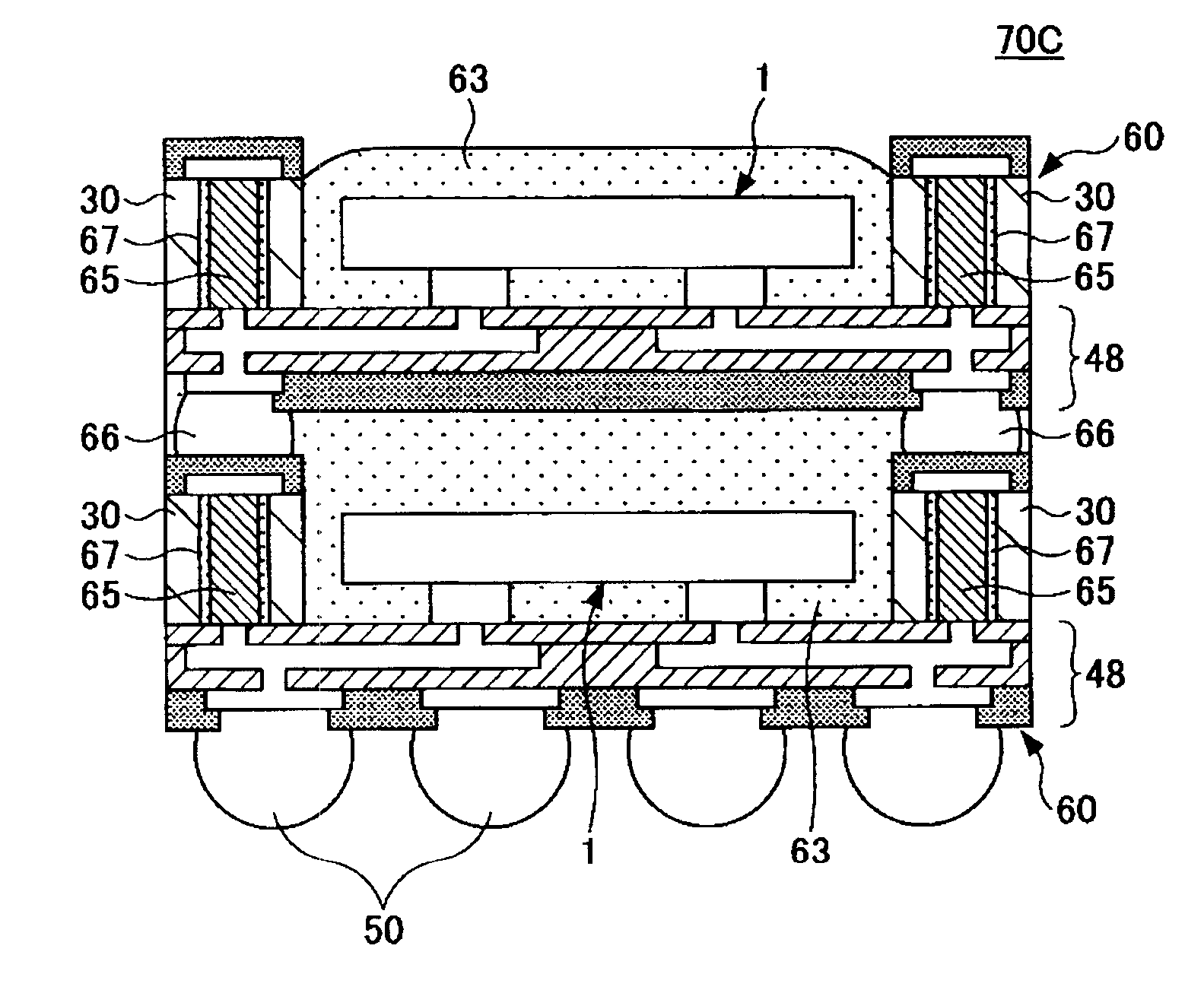
[0038]FIG. 5A to FIG. 10C are views showing a method of manufacturing a wiring substrate as an embodiment of the present invention along with manufacturing steps. In the method of manufacturing the wiring substrate according to the present embodiment, one feature resides in that the wiring substrate is manufactured in a state that a dummy chip is arranged instead of the chip component, as described later. For this reason, prior to the explanation of the method of manufacturing the wiring substrate using FIG. 5A to FIG. 10C, a method of manufacturing a dummy chip will be explained with reference to FIG. 3A to FIG. 4C hereunder.

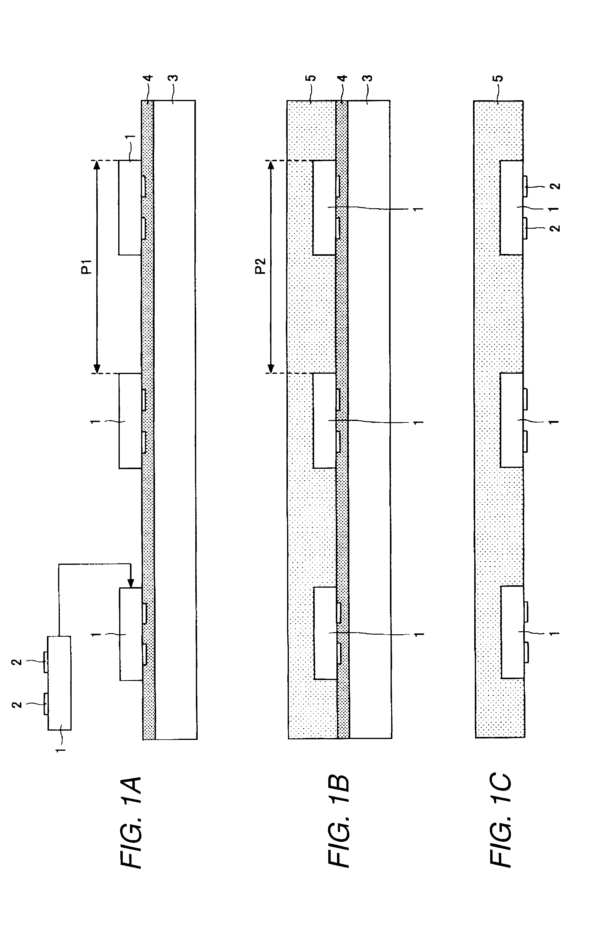
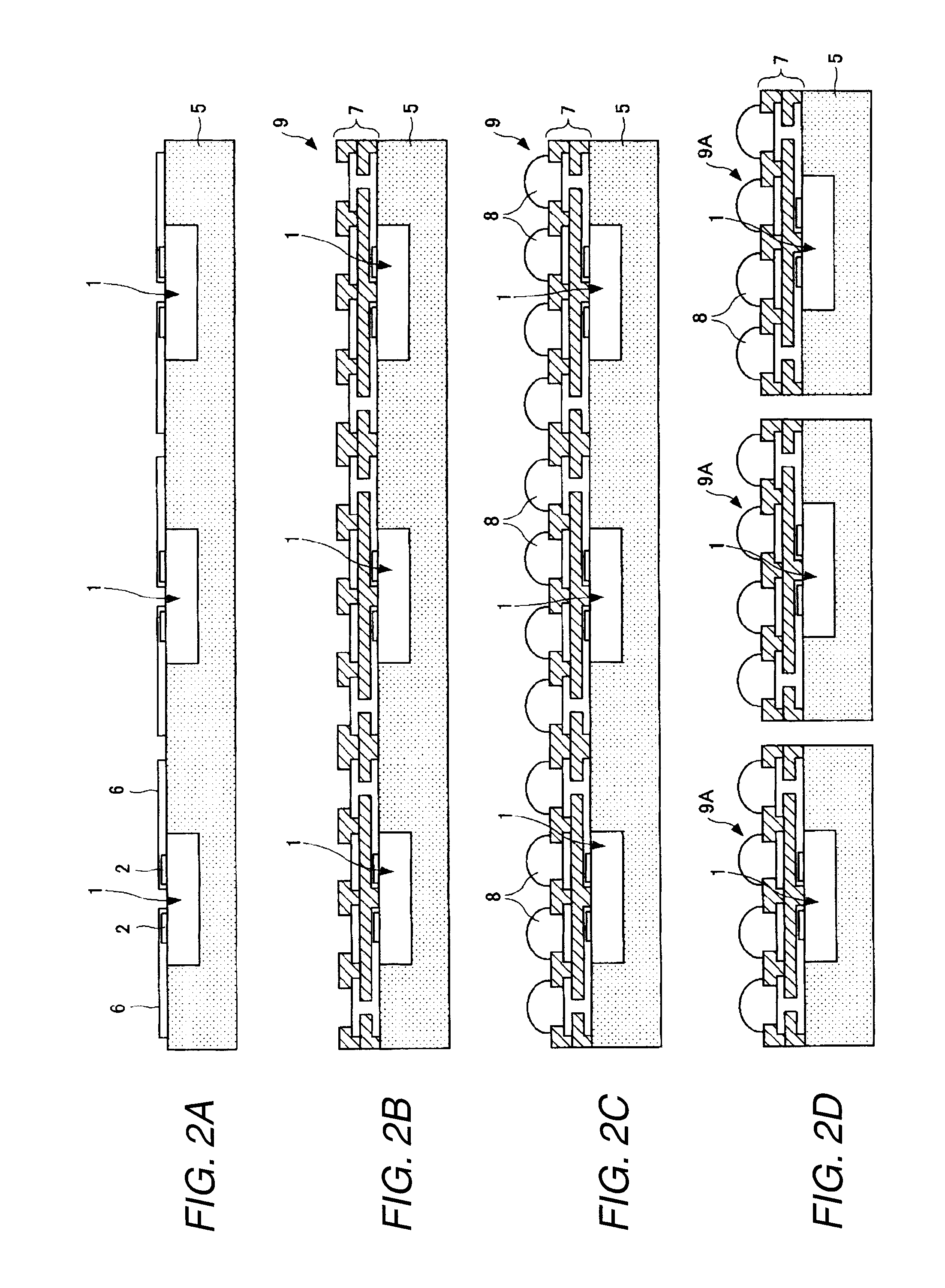
[0039]In order to manufacture a dummy chip 20, as shown in FIG. 3A, first a dummy chip substrate 10 is prepared. In the present embodiment, a silicon wafer is employed as the dummy chip substrate 10.

[0040]In the present embodiment, the sem...


PUM


Abstract

There are provided a step of preparing a dummy chip, a step of forming a cavity in a stiffener substrate, a step of providing a second tape base member on one surface of the stiffener substrate, a step of inserting the dummy chip into the cavity to provide the dummy chip on the second tape base member, a step of sealing the stiffener substrate and the dummy chip with a sealing resin, a step of removing the second tape base member and forming a build-up wiring layer on a surface from which the second tape base member is removed, a step of removing the sealing resin; and a step of peeling the dummy chip from the build-up wiring layer.

Description

TECHNICAL FIELD[0001]The present disclosure relates to a method of manufacturing a wiring substrate and a method of manufacturing an semiconductor device and, more particularly, a method of manufacturing a wiring substrate having a structure in which a chip is built and a method of manufacturing an semiconductor device using the wiring substrate.RELATED ART[0002]In recent years, along with the needs such as higher performance, size reduction, and the like of the electronic apparatus, the high-density packaging of the electronic component incorporated into the electronic apparatus is proceeding swiftly. Such a method has been employed that a substrate and a semiconductor chip are manufactured by the separate step respectively and then the semiconductor chip is flip-chip mounted onto the substrate that is manufactured individually.[0003]However, it is difficult to achieve sufficiently a higher performance and a size reduction by this method. Therefore, a substrate constructed by insta...

Claims


Application Information

Patent Timeline
IPC IPC(8): B32B37/00
CPCH01L21/4857H01L21/568H01L23/5389H01L23/544H01L24/11H01L24/81H01L24/96H01L24/97H01L25/105H01L2223/54473H01L2224/04105H01L2224/11003H01L2224/13099H01L2224/16H01L2224/20H01L2224/81193H01L2224/81801H01L2224/97H01L2924/01022H01L2924/01029H01L2924/01074H01L2924/01078H01L2924/10157H01L2924/15311H01L2924/15331H01L2924/16195H01L2924/30107H01L21/6835H01L2224/12105H01L2224/0401H01L2225/1058H01L2924/01005H01L2924/01006H01L2924/01033H01L2924/014H01L24/19H01L2225/1035H01L2224/82H01L2224/16238H01L2924/15153H01L2924/181H01L2924/3511H01L2924/00
Inventor SUNOHARA, MASAHIROMURAYAMA, KEIHIGASHI, MITSUTOSHISAKAGUCHI, HIDEAKI
Owner SHINKO ELECTRIC IND CO LTD
Why Eureka
Try Eureka