Laser welding structure and laser welding method
a laser welding and laser welding technology, applied in the field of laser welding structure and laser welding method, can solve the problems of crack generation at the recrystallization, difficult absorption of laser light energy by copper alloy, and prone to laser light irradiation
- Summary
- Abstract
- Description
- Claims
- Application Information
AI Technical Summary
Benefits of technology
Problems solved by technology
Method used
Image

Examples
first embodiment
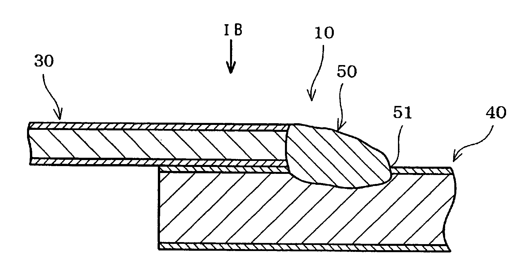
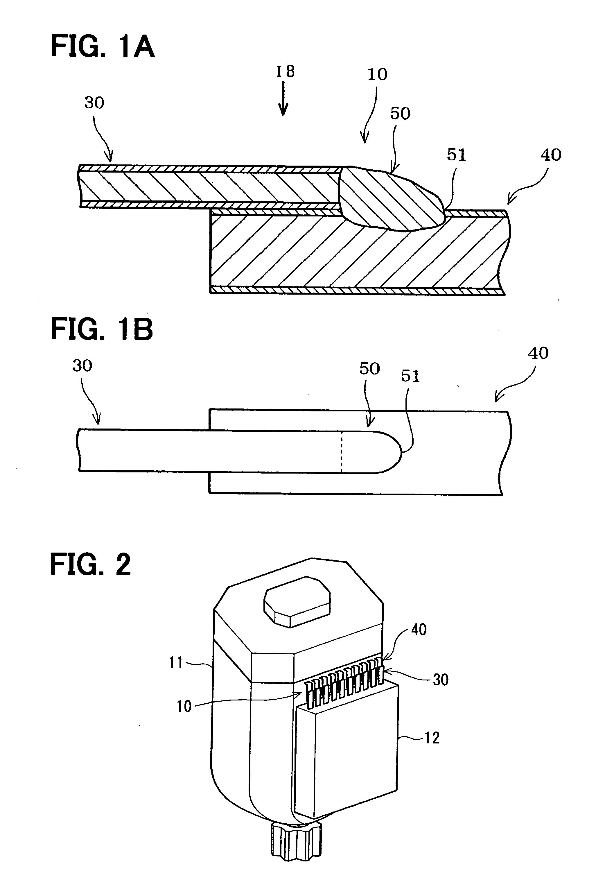
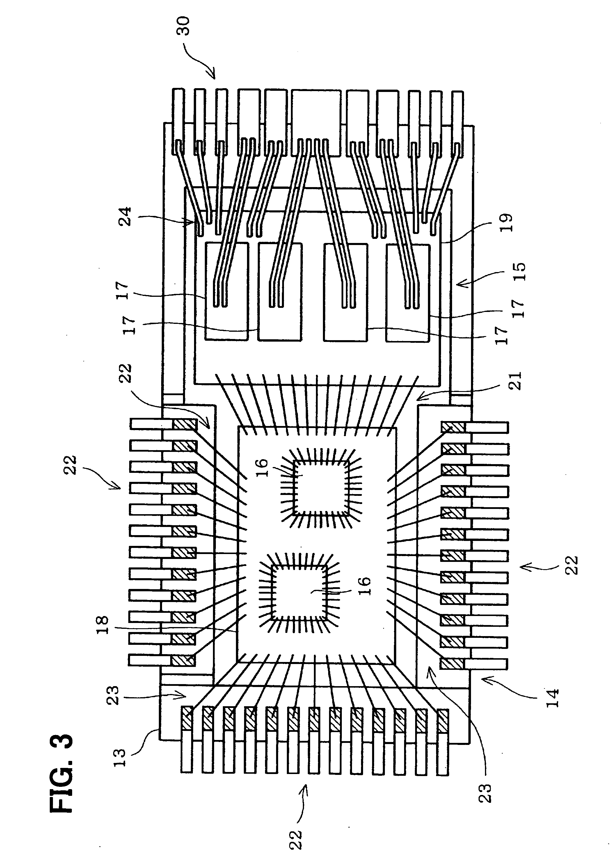
[0037]A laser welding portion 10 to which a laser molding structure according to a first embodiment of the present invention is illustrated in FIG. 1A and FIG. 1B. The laser welding portion 10 can be applied to, for example, a mold integrated circuit device 12 that is integrated with a motor 11 as illustrated in FIG. 2. The mold integrated circuit device 12 includes a processing section 14 and a control section 15 sealed by a resin package 13, as illustrated in FIG. 3. In the processing section 14, integrated circuit chips 16 each having a plurality of pins are disposed. The integrated circuit chips 16 include, for example, a central processing unit (CPU) and a memory for configurating a microcomputer. In the control section 15, power elements 17 such as a power metal-oxide semiconductor field-effect transistor (power MOSFET) are disposed. The integrated circuit chips 16 in the processing section 14 are mounted on a substrate 18. The power elements 17 in the control section 15 are m...
second embodiment
[0051]A laser welding structure according to a second embodiment will be described with reference to FIG. 7. In the present embodiment, the plating layer 32 is formed on the end surface 33 of the lead 30 in addition to the two surfaces of the lead body 31 in the thickness direction and the two surfaces of the lead body 31 in the width direction. By providing the plating layer 32 on the end surface 33 of the lead 30, the area of the plating layer 32 having a low melting point increases. Thereby, when the laser light is irradiated, the portion that becomes the seed of melting can be easily formed at the plating layer 32. Thus, the welding part 50 can be formed effectively. When the plating layer 32 is provided on the end surface 33 of the lead 30, the plating layer 32 may be formed after the lead 30 is punched out from a frame (not shown). Before punching out, the plating layer 32 may be formed on each of the surfaces of the lead body 31 except for the end surface 33.
third embodiment
[0052]A laser welding structure according to a third embodiment of the present invention will be described with reference to FIG. 8. In the present embodiment, the lead 30 has a chamfered part 34. The chamfered part 34 is formed by cutting edges of the end surface 33 of the lead 30. That is, at the end portion of the lead 30, a periphery of the irradiated area 61 is cut on a plane. In FIG. 8, the welding part 50 formed by irradiating the laser light is illustrated by a dashed line. By providing the chamfered part 34, the end 51 of the welding part 50 melted at the irradiation of the laser light becomes a shape similar to the end surface 33 of the lead 30. Thus, the end 51 of the welding part 50 can be the circular arc shape more easily. As a result, a generation of a crack at the welding part 50 can be reduced. The chamfered part 34 can be formed when the lead 30 is punched out from the frame.
PUM
| Property | Measurement | Unit |
|---|---|---|
| Thickness | aaaaa | aaaaa |
| Diameter | aaaaa | aaaaa |
| Shape | aaaaa | aaaaa |
Abstract
Description
Claims
Application Information
 - Generate Ideas
- Intellectual Property
- Life Sciences
- Materials
- Tech Scout
- Unparalleled Data Quality
- Higher Quality Content
- 60% Fewer Hallucinations
Browse by: Latest US Patents, China's latest patents, Technical Efficacy Thesaurus, Application Domain, Technology Topic, Popular Technical Reports.
© 2025 PatSnap. All rights reserved.Legal|Privacy policy|Modern Slavery Act Transparency Statement|Sitemap|About US| Contact US: help@patsnap.com