Process to make metal oxide thin film transistor array with etch stopping layer

a thin film transistor and etching technology, applied in the direction of transistors, electrical devices, semiconductor devices, etc., can solve the problem of negative affecting the performance of

Active Publication Date: 2009-09-24
APPLIED MATERIALS INC
View PDF99 Cites 67 Cited by
  • Summary
  • Abstract
  • Description
  • Claims
  • Application Information

AI Technical Summary

Benefits of technology

[0010]The present invention generally relates to TFTs and methods of making TFTs. The active channel of the TFT may comprise one or more metals selected from the group consisting of zinc, gallium, tin, indium, and cadmium. The active channel may also comprise nitrogen and oxygen. To protect the active channel during source-drain electrode patterning, an etch stop layer may be deposited over the active layer. The etch stop layer prevents the active channel from being exposed to the plasma used to define the source and drain electrodes. The etch stop layer and the source and drain electrodes may be used as a mask when wet or dry etching the active material layer that is used for the active channel.
[0011]In one embodiment, a thin film transistor formation method comprises depositing and patterning a gate electrode over a substrate, depositing a gate dielectric layer over the gate electrode, and depositing a semiconductive active layer over the gate dielectric layer. The active layer may comprise oxygen, nitrogen, and one or more elements selected from the group consisting of zinc, indium, cadmium, gallium, and tin. The active layer may be doped. The method also comprises depositing an etch stop layer over the active layer, forming a first mask over the etch stop layer, patterning the etch stop layer and removing the first mask. The method also comprises depositing a metal layer over the etch stop layer, forming a second mask over the metal layer, etching the metal layer to define a source electrode and a drain electrode and removing the second mask

Problems solved by technology

Plasma exposure of the active material layer ma

Method used


Image

  • Process to make metal oxide thin film transistor array with etch stopping layer
  • Process to make metal oxide thin film transistor array with etch stopping layer
  • Process to make metal oxide thin film transistor array with etch stopping layer

Examples


Embodiment Construction

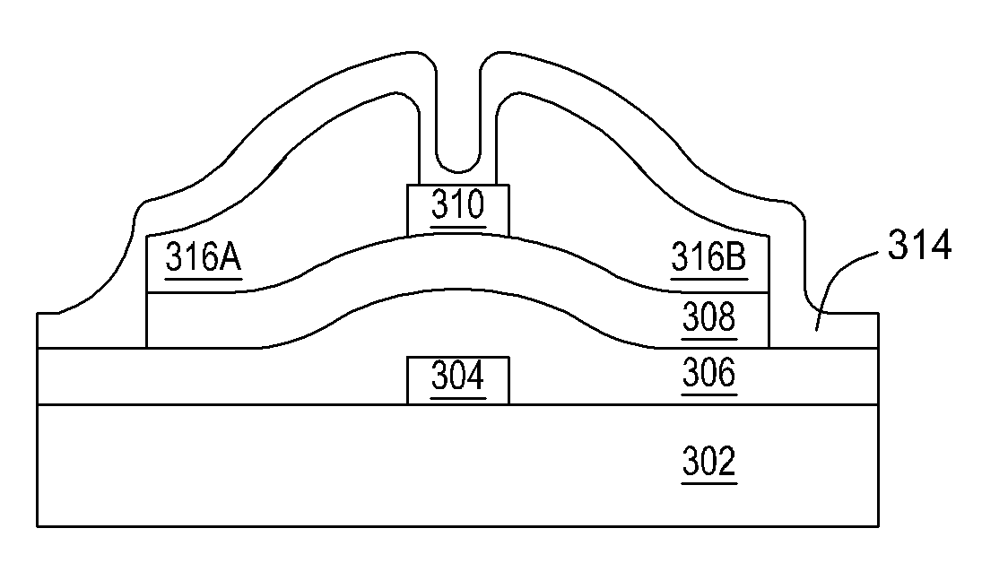
[0020]The present invention generally relates to TFTs and methods of making TFTs. The active channel of the TFT may comprise one or more metals selected from the group consisting of zinc, gallium, tin, indium, and cadmium. The active channel may or may not be doped. The active channel may also comprise nitrogen and oxygen. To protect the active channel during source-drain electrode patterning, an etch stop layer may be deposited over the active layer. The etch stop layer prevents the active channel from being exposed to the plasma used to define the source and drain electrodes. The etch stop layer and the source and drain electrodes may be used as a mask when wet etching the active material layer that is used for the active channel.

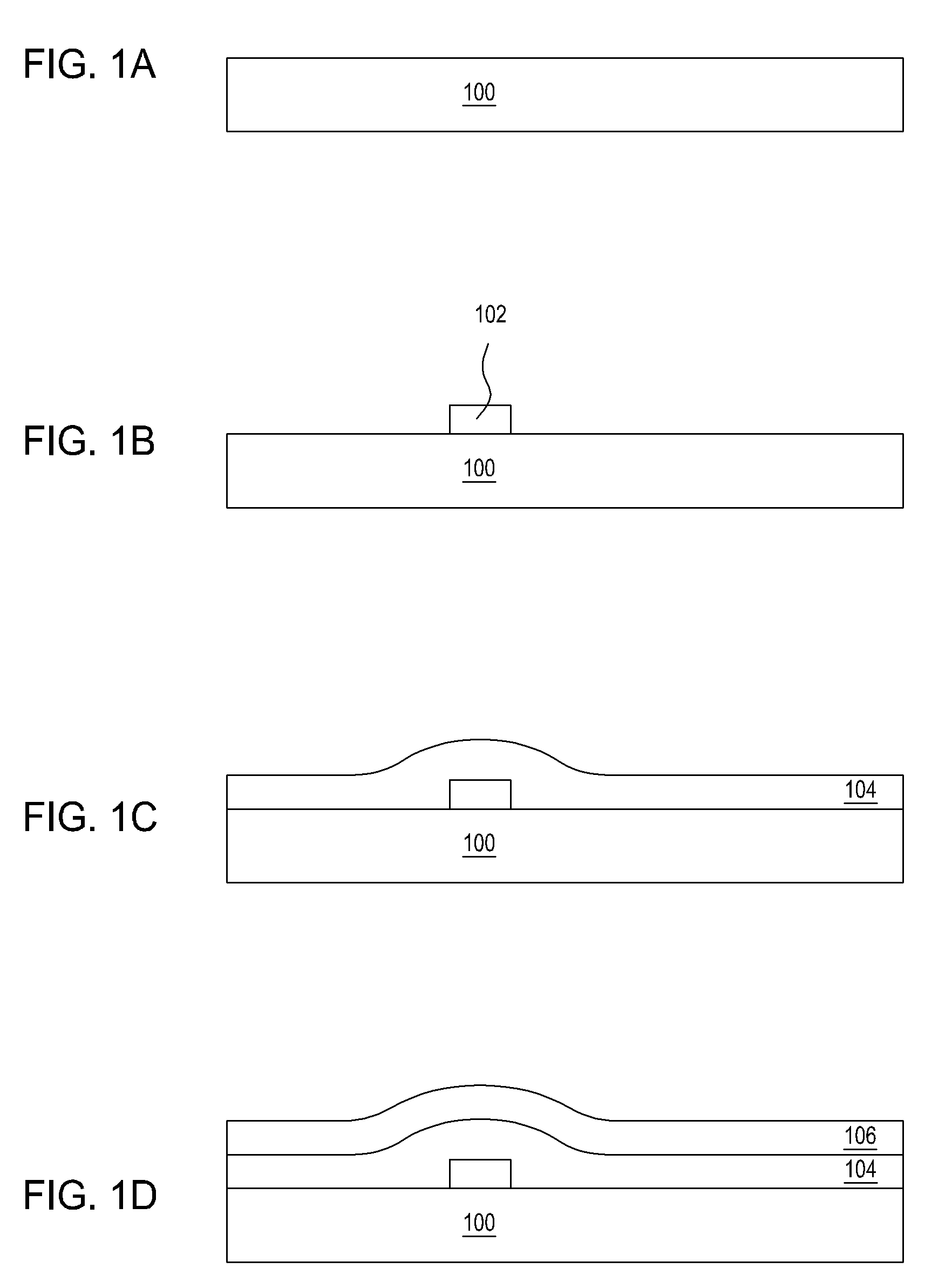
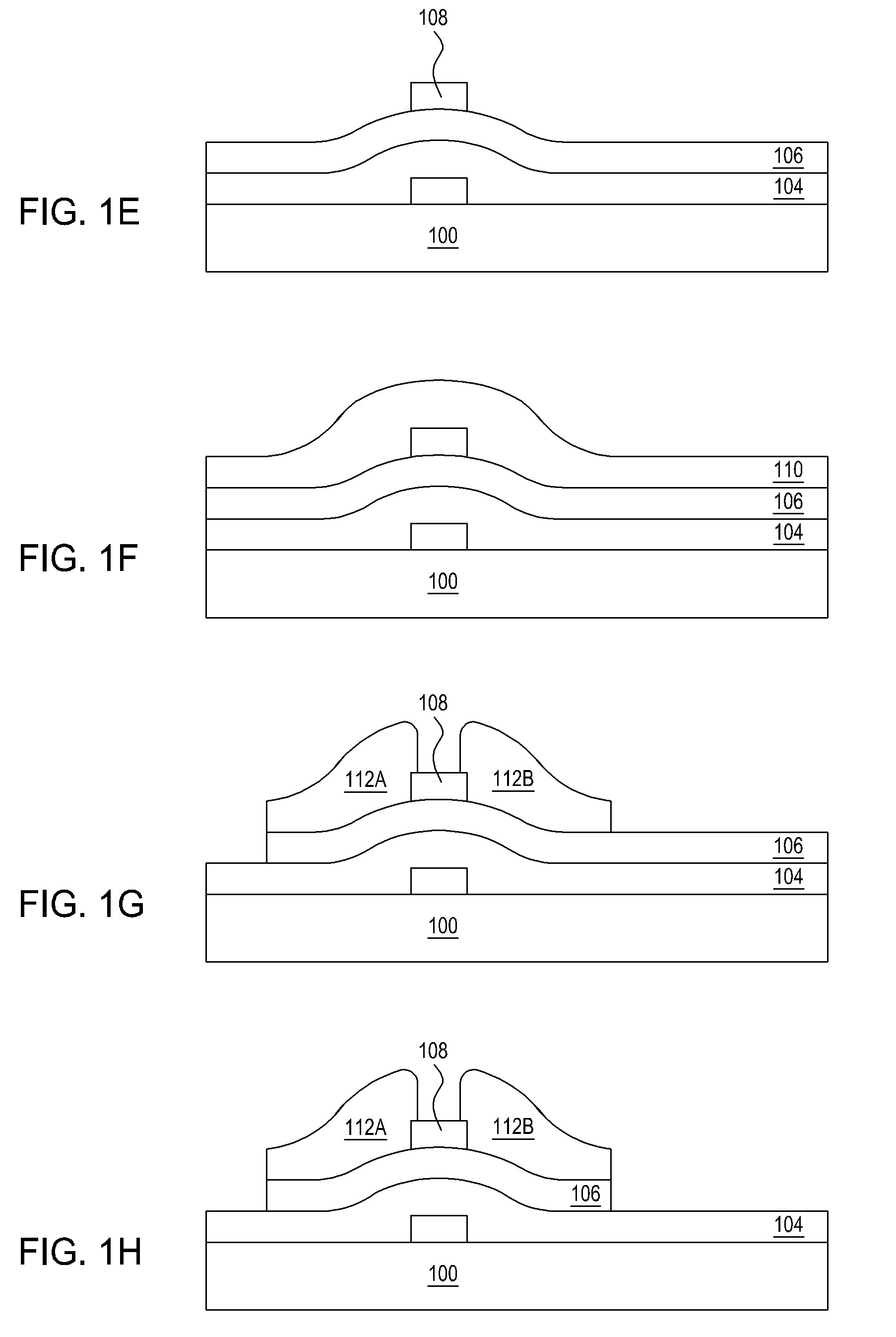
[0021]FIGS. 1A-1J show a TFT in various stages of processing according to one embodiment of the invention. In FIG. 1A, a substrate 100 is shown. In one embodiment, the substrate 100 may comprise glass. In another embodiment, the substrate 100 may comprise...


PUM


Abstract

The present invention generally relates to thin film transistors (TFTs) and methods of making TFTs. The active channel of the TFT may comprise one or more metals selected from the group consisting of zinc, gallium, tin, indium, and cadmium. The active channel may also comprise nitrogen and oxygen. To protect the active channel during source-drain electrode patterning, an etch stop layer may be deposited over the active layer. The etch stop layer prevents the active channel from being exposed to the plasma used to define the source and drain electrodes. The etch stop layer and the source and drain electrodes may be used as a mask when wet etching the active material layer that is used for the active channel.

Description

CROSS-REFERENCE TO RELATED APPLICATIONS[0001]This application claims benefit of U.S. provisional patent application Ser. No. 61 / 038,289 (Attorney Docket No. APPM / 013123L), filed Mar. 20, 2008, which is herein incorporated by reference.BACKGROUND OF THE INVENTION[0002]1. Field of the Invention[0003]Embodiments of the present invention generally relate to a thin film transistor (TFT) fabrication method and a TFT produced by the method.[0004]2. Description of the Related Art[0005]Current interest in TFT arrays is particularly high because these devices may be used in liquid crystal active matrix displays (LCDs) of the kind often employed for computer and television flat panels. The LCDs may also contain light emitting diodes (LEDs) for back lighting. Further, organic light emitting diodes (OLEDs) have been used for active matrix displays, and these OLEDs utilize TFTs for addressing the activity of the displays.[0006]TFTs made with amorphous silicon as the active material have become th...

Claims


Application Information

Patent Timeline
IPC IPC(8): H01L29/786H01L21/18H01L21/336
CPCH01L29/7869
Inventor YE, YAN
Owner APPLIED MATERIALS INC
Why Eureka
Try Eureka