Flip chip interconnection system

a chip and interconnection technology, applied in the direction of printed circuit manufacturing, printed circuit aspects, conductive material removal by irradiation, etc., can solve the problems of inconvenient design of solder mask openings that only leave wettable pads exposed, inconvenient installation of solder masks, and long time-consuming for those skilled in the art to solv

Active Publication Date: 2009-09-24
STATS CHIPPAC LTD
View PDF30 Cites 49 Cited by
  • Summary
  • Abstract
  • Description
  • Claims
  • Application Information

AI Technical Summary

Problems solved by technology

If wettable pads are not defined on the substrate, the solder would wet the substrate uncontrollably resulting in inconsistent formation or failure of the solder bumps and implicitly of the integrated circuit die.
To design the openings in the solder mask that only leave the wettable pads exposed becomes difficult because of the increasingly tight tolerances.
Solutions to these problems have been long sought but prior developments have not taught or suggested any solutions and, thus, solutions to these problems have long eluded those skilled in the art.

Method used


Image

  • Flip chip interconnection system
  • Flip chip interconnection system
  • Flip chip interconnection system

Examples


first embodiment

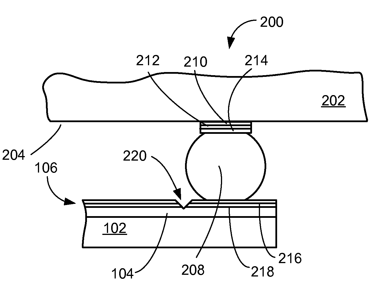
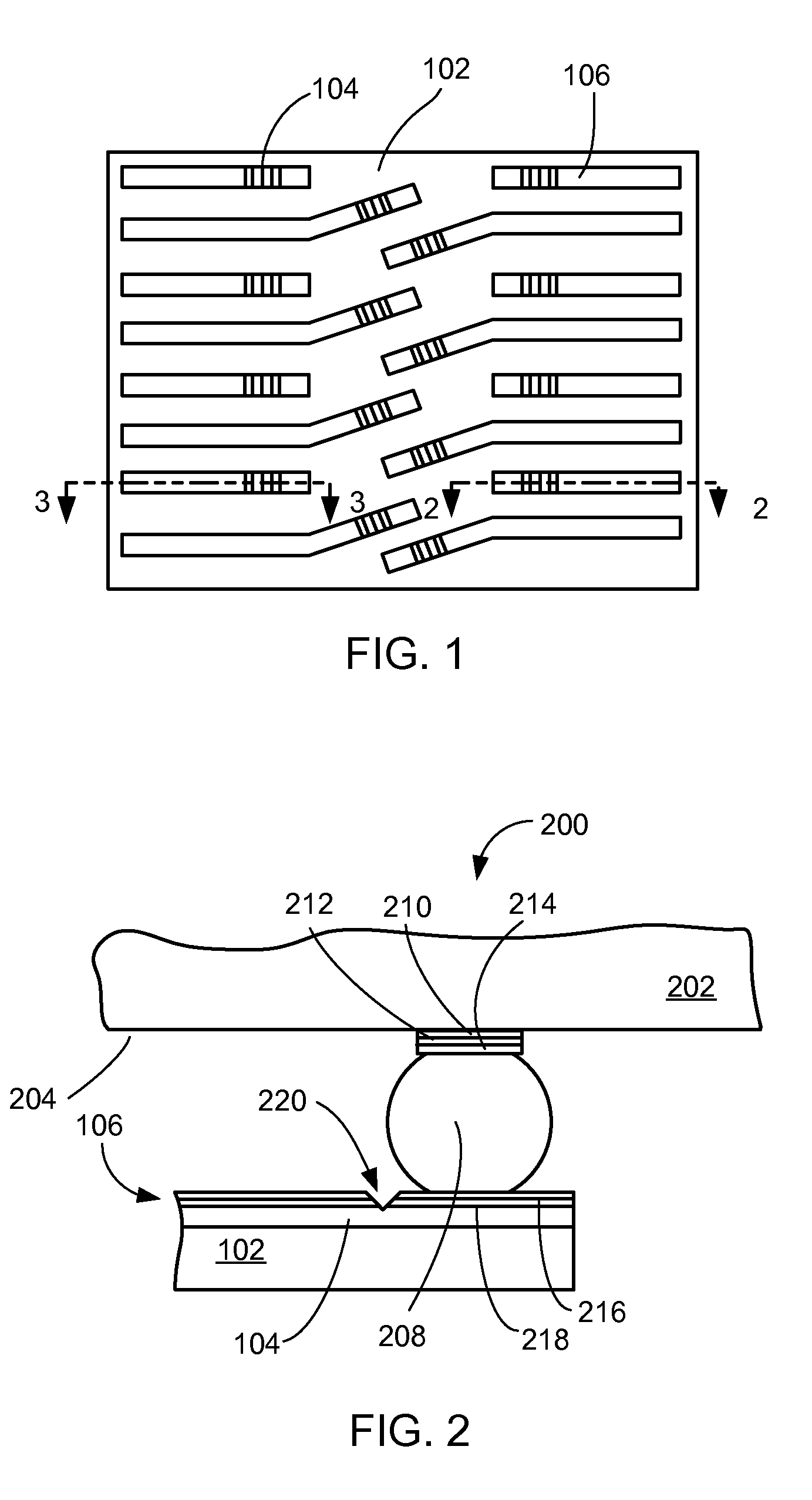
[0039]Referring now to FIG. 2, therein is shown a close up of a cross-sectional view of a flip chip interconnection system 200 along line 2-2 of FIG. 1 in the present invention.

[0040]The flip chip interconnection system 200 includes a flip chip 202 having an active side 204, a conductive bump 208, such as a solderable conductive interconnect, the substrate 102 with the conductive trace 104, and the protective coating 106.

[0041]The flip chip 202 may be electrically and mechanically coupled to the substrate 102 using a flip chip interconnect, such as the conductive bump 208. The conductive bump 208 can be of solder materials such as lead, tin, and antimony.

[0042]To attach the conductive bump 208 to the flip chip 202, an under bump metallization is applied on the flip chip 202. The under bump metallization consists of an adhesion layer 210, such as titanium tungsten, for good adhesion to the flip chip 202, a barrier layer 212, such as a gold, to limit the diffusion of solder into the u...

second embodiment

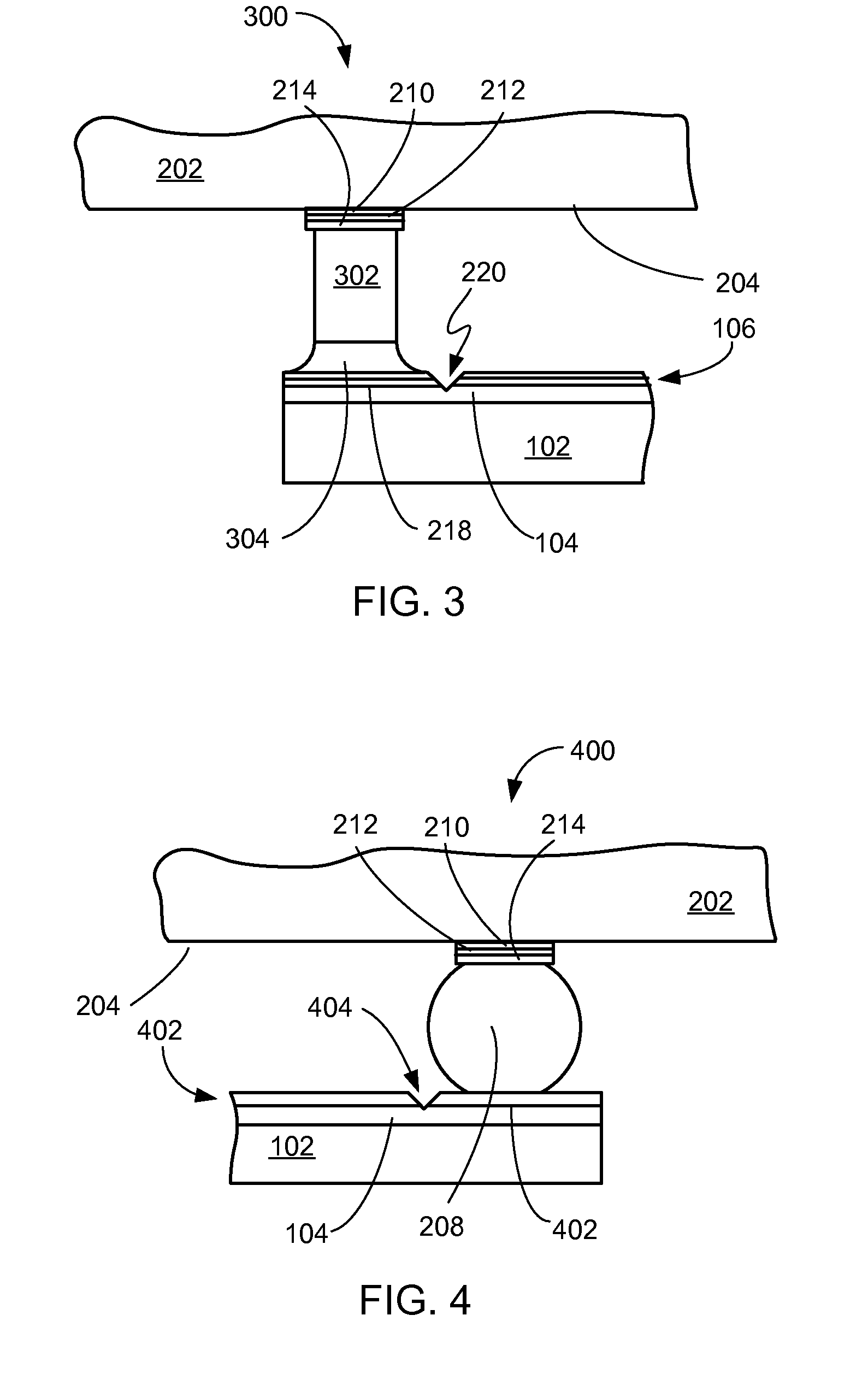
[0048]Referring now to FIG. 3, therein is shown a close up of a cross-sectional view of a flip chip interconnection system 300 along line 2-2 of FIG. 1 in the present invention.

[0049]The flip chip interconnection system 300 includes the flip chip 202 having the active side 204, conductive pillars 302, and the substrate 102 with the conductive trace 104 and the protective coating 106.

[0050]The flip chip 202 may be electrically and mechanically coupled to the substrate 102 using a flip chip interconnect, such as a conductive pillar 302. The conductive pillar 302 can be of a material, such as copper. However, the conductive pillar 302, when made of copper, can have intermetallic issues and have a tendency to oxidize in the presence of some alloys.

[0051]It has been found that the conductive pillar 302 should have a solder tip 304 of lead, tin, or antimony to eliminate the impact of oxidation and intermetallics that may lead to reliability issues.

[0052]The conductive pillar 302 is often ...

third embodiment

[0063]Referring now to FIG. 4, therein is shown a close up of a cross-sectional view of a flip chip interconnection system 400 similar to FIG. 2 in the present invention.

[0064]The flip chip interconnection system 400 includes the flip chip 202 having the active side 204, the conductive bump 208, the substrate 102 with the conductive trace 104 and a protective coating 402.

[0065]The flip chip 202 may be electrically and mechanically coupled to the substrate 102 using a flip chip interconnect, such as the conductive bump 208. The conductive bump 208 can be of solder materials such as lead, tin, and antimony.

[0066]To attach the conductive bump 208 to the flip chip 202, an under bump metallization is applied on the flip chip 202. The under bump metallization consists of the adhesion layer 210, such as titanium tungsten, for good adhesion to the flip chip 202, the barrier layer 212, such as a gold, to limit the diffusion of solder into the underlying material, and the solder wettable laye...


PUM


Abstract

A flip chip interconnection system includes: providing a conductive lead coated with a protective coating; forming a groove through the protective coating to the conductive lead for controlling solder position on a portion of the conductive lead; and attaching a flip chip having a solderable conductive interconnect to the portion of the conductive lead.

Description

TECHNICAL FIELD[0001]The present invention relates to a method of connecting an integrated circuit chip to a substrate. More particularly, the invention relates to a flip chip interconnection system.BACKGROUND ART[0002]Portable electronics products such as cellular phone, PDA, DVC, DSC acquire multi-functions in an accelerating speed, and in such condition the miniaturization and the weight reduction is essential for these products to be accepted by the market, and thus LSI (large scale integration) having higher integration level are necessary to satisfy these needs.[0003]On the other hand, more user-friendly and convenient products are also desired for these electronics products by the market, and thus LSI having multiple functions and higher performances are needed for utilizing these products. For this reason, number of inputs / outputs (I / O) increases as the level of the integration of LSI increases, while the requirement for miniaturizing the package itself becomes considerable....

Claims


Application Information

Patent Timeline
Patent Type & Authority Applications(United States)
IPC IPC(8): H01L23/48H01L21/60
CPCH01L23/49838H01L2224/10175H01L24/16H01L24/81H01L2224/1308H01L2224/13082H01L2224/13111H01L2224/13116H01L2224/1312H01L2224/13147H01L2224/16H01L2224/81801H01L2924/01079H01L2924/14H05K3/027H05K3/244H05K3/3452H05K2201/10674H05K2201/2081H05K2203/0361H01L24/12H01L2224/1415H01L2224/81191H01L2924/01327H01L2924/00013H01L2924/00014H01L2224/13099H01L2224/29099H01L2224/0508H01L2224/05568H01L2224/05023H01L2224/05001H01L2224/05144H01L2224/05655H01L2224/0615H01L24/05
Inventor KIM, OH HANKIM, KYUNG MOON
Owner STATS CHIPPAC LTD
Why Eureka
Try Eureka