Flip-chip assembly and manufacture method thereof

A flip-chip and assembly technology, which is applied in semiconductor/solid-state device manufacturing, electrical components, semiconductor devices, etc., can solve the problems of half-break chips affecting reliability, etc., and achieve large-scale low-cost, reliable and interconnected, good The effect of thermal conductivity

Inactive Publication Date: 2009-10-28
CHENGDU MONOLITHIC POWER SYST
View PDF0 Cites 5 Cited by
  • Summary
  • Abstract
  • Description
  • Claims
  • Application Information

AI Technical Summary

Problems solved by technology

[0006] The purpose of the present invention is to solve the problem that the existing flip-chip interconnection member adopting long copper terminal posts and its manufacturing method may cause the half-off chip to suffer thermally induced mechanical stress to affect its reliability. generated at the base layer or along the body of the interconnecting member

Method used


Image

  • Flip-chip assembly and manufacture method thereof
  • Flip-chip assembly and manufacture method thereof
  • Flip-chip assembly and manufacture method thereof

Examples


Embodiment Construction

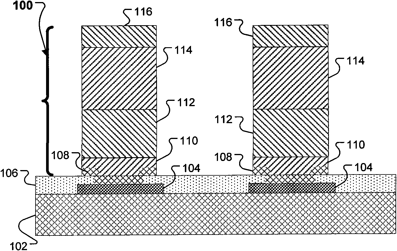
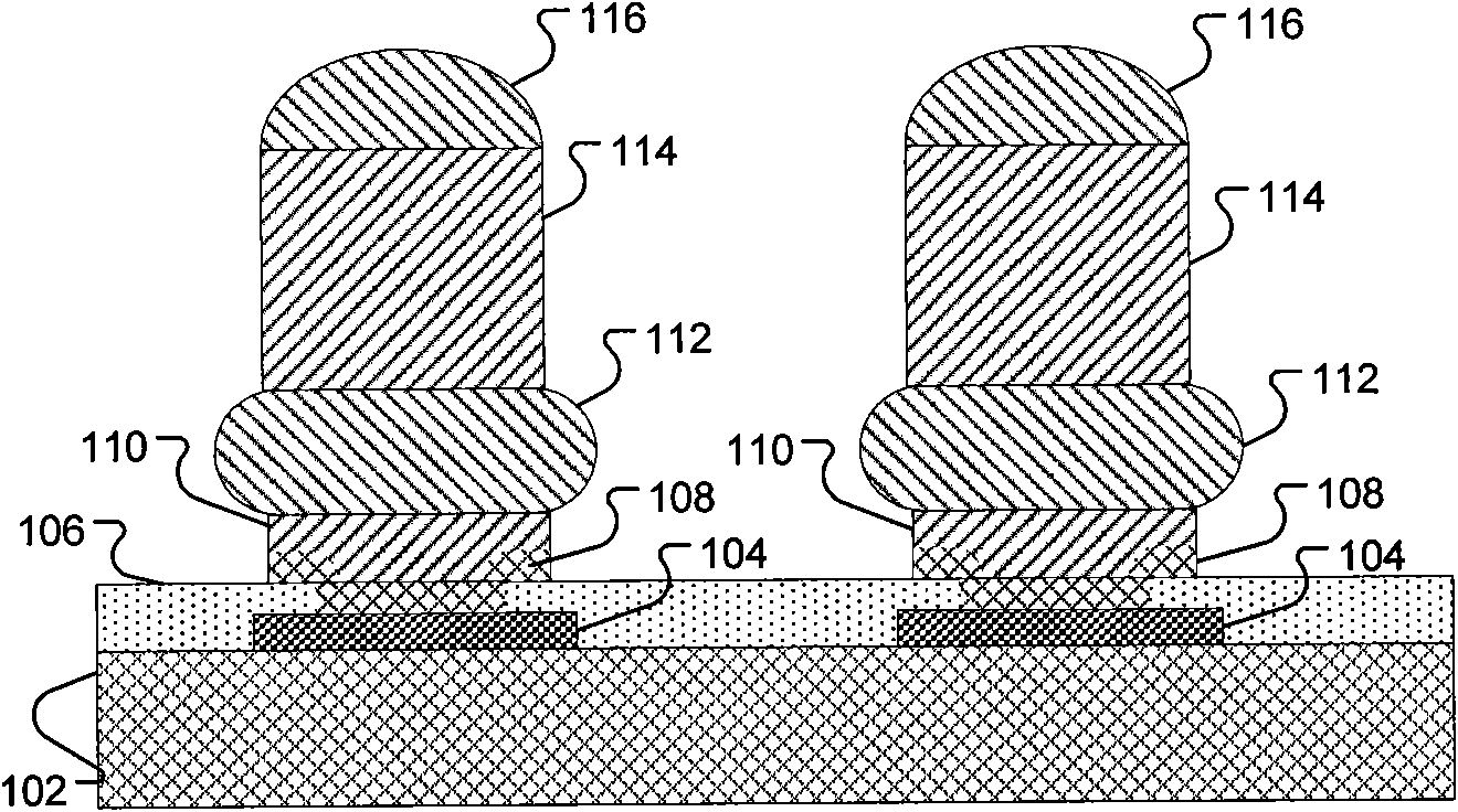
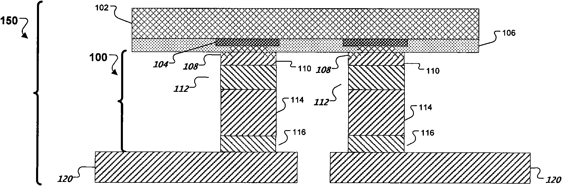
[0020] Embodiments disclosed herein relate to a flip chip interconnection structure electrically connecting a semiconductor chip to a support substrate, and a method of manufacturing the flip chip interconnection structure. The interconnection member has the following functions in the flip-chip assembly. Electrically, the interconnection member can provide a conductive path from the chip to the supporting substrate; the interconnecting member can also provide a thermal conduction path to transfer the heat of the chip to the supporting substrate. ; In addition, the interconnection member can also mechanically attach part or all of the chip to the support substrate; in addition, the interconnection member can also be used as a spacer to prevent electrical contact between the chip and the conductor on the support substrate, and at the same time as a Short leads with mechanical stress between die and substrate.

[0021] Figure 1A is a cross-sectional view of a flip-chip interconn...


PUM


Abstract

The invention discloses a flip-chip assembly and manufacture method thereof. Various aspects can be implemented for providing flip-chip interconnect structures for connecting or mounting semiconductor chips to supporting substrates, such as cards, circuit boards, carriers, lead frames, and the like. In general, one aspect can be a method of providing a flip-chip interconnect structure that includes providing a semiconductor work piece that includes one or more bond pads. The method also includes depositing a first non-reflowable layer that has a first melting temperature higher than a predetermined first reflow temperature. The method further includes depositing a reflowable stress relief layer that reflows at the predetermined first reflow temperature. The method additionally includes depositing a second non-reflowable layer that has a second melting temperature higher than the predetermined first reflow temperature such that the deposited reflowable stress relief layer is between the first and the second non-reflowable layers.

Description

technical field [0001] The invention discloses a flip-chip welding structure, in particular to a flip-chip interconnection for connecting or mounting semiconductor workpieces, such as devices, bare chips, wafers, and chips (hereinafter collectively referred to as "semiconductor chips") Component, supporting (eg packaged or interconnected) substrate such as card board, circuit board, carrier, lead frame, etc. Background technique [0002] Unlike wire bonding, in which the face-up semiconductor chip is electrically connected to each pad of the semiconductor chip by wires, flip-chip bonding uses a conductive interconnect (such as solder bumps) to connect the face-down semiconductor chip. dots or copper terminal posts) are electrically connected to each pad of the semiconductor chip. In addition to semiconductor chips, flip chip bonding can also be used for other components such as passive filters, detector arrays and MEMS devices. [0003] Temperature variations during semico...

Claims


Application Information

Patent Timeline
Patent Type & Authority Applications(China)
IPC IPC(8): H01L23/485H01L21/60
CPCH01L2924/01082H01L2924/01049H01L2224/81801H01L2224/13109H01L2924/01322H01L2224/13609H01L2924/01029H01L2924/00013H01L2224/13147H01L2924/01022H01L24/11H01L2924/014H01L2924/01013H01L2924/01024H01L2224/8101H01L2924/01047H01L24/81H01L2924/01079H01L2224/1308H01L2224/13155H01L24/16H01L2924/19042H01L2924/01005H01L2924/01033H01L2924/01006H01L2224/13084H01L2924/01074H01L2924/01078H01L2224/13111H01L24/12H01L2924/1461H01L2224/11462H01L2224/05027H01L2224/05022H01L2224/05001H01L2224/05572H01L2224/051H01L2224/056H01L2224/05611H01L2224/05655H01L2224/81011H01L24/13H01L24/06H01L24/05H01L2224/13017H01L2924/00014H01L2924/01083H01L2224/13099H01L2924/00
Inventor 蒋航
Owner CHENGDU MONOLITHIC POWER SYST
Why Eureka
Try Eureka