Analog-to-digital converter, analog-to-digital converting method, solid-state image pickup device, and camera system

an analog-to-digital converter and digital converter technology, applied in the field of analog-to-digital converters, solid-state image pickup devices, camera systems, etc., can solve the problems of difficult to improve the precision of ad conversion, adc becomes outside the ad range (overflow), and the offset voltage generated is difficult to be determined. , to achieve the effect of high precision, improved conversion processing speed and extended dynamic rang

Active Publication Date: 2009-09-24
SONY CORP
View PDF7 Cites 23 Cited by
  • Summary
  • Abstract
  • Description
  • Claims
  • Application Information

AI Technical Summary

Benefits of technology

[0059]According to the embodiments of the present invention, the dynamic range can be extended with high precision, without the ADC becoming outside the AD range (overflow), and the speed of conversion processing can be increased.

Problems solved by technology

In this case, whether an offset voltage has been generated or not is difficult to be determined unless the ADC deviates from the input range once.
Therefore, there is a disadvantage that the ADC becomes outside the AD range (overflow) at least once.
With this method, however, it is difficult to improve the precision of AD conversion.
In this case, since it is difficult to make the slope of a P-phase reference signal equivalent to that of a D-phase reference signal, disadvantageously, the precision of correlated double sampling (CDS) is dropped, and accordingly, CDS itself becomes difficult.
In practice, it is difficult to make each reference signal have the same slope.
Therefore, the reference signals have different slopes and are not combined well.
Disadvantageously, it is difficult to perform correction at a subsequent stage.

Method used


Image

  • Analog-to-digital converter, analog-to-digital converting method, solid-state image pickup device, and camera system
  • Analog-to-digital converter, analog-to-digital converting method, solid-state image pickup device, and camera system
  • Analog-to-digital converter, analog-to-digital converting method, solid-state image pickup device, and camera system

Examples


first embodiment

[0091]FIG. 4 is a block diagram showing an exemplary structure of an ADC according to a first embodiment.

[0092]Referring to FIG. 4, the ADC 200 is shown. Also, the comparator 151 shown in FIG. 3 is denoted by reference numeral 210.

[0093]The ADC 200 shown in FIG. 4 includes the comparator 210 (151), a counter 220 that counts a comparison time of the comparator 210, a control circuit 230 that monitors an output of the comparator 210, a voltage generating circuit 240 that generates a DC voltage in accordance with the monitoring result obtained by the control circuit 230, a capacitor C1 connected to an analog-signal (Vsig) input terminal of the comparator 210, a capacitor C2 connected to an output side of the voltage generating circuit 240, an analog adder 250 that adds an analog signal Vsig via the capacitor C1 and a DC signal via the capacitor C2, and a digital-signal correcting circuit 260.

[0094]In the structure shown in FIG. 4, the analog adder 250 is a wired-OR gate.

[0095]The compa...

second embodiment

[0161]FIG. 9 is a block diagram showing an exemplary structure of an ADC according to a second embodiment.

[0162]An ADC 200C according to the second embodiment includes, besides the structure of the ADC 200 according to the first embodiment, which is shown in FIG. 4, a memory 270 whose initial value can be set. In accordance with a signal S230 from the control circuit 230, different initial values of the counter 220 can be selected.

[0163]FIG. 10 is a timing chart for illustrating the operation of the ADC shown in FIG. 9.

[0164]Hereinafter, the operation of the ADC shown in FIG. 9 will be described with reference to FIG. 10.

Operation

[0165]In a period A, a signal voltage Vsig, a voltage Va from the voltage generating circuit 240, and a reference wave Vref are set to fixed voltages. An output of the comparator 210 is determined by the control circuit 230, and the output voltage Va of the voltage generating circuit 240 is switched.

[0166]When the output of the comparator 210 is 0 V, the co...

third embodiment

[0209]FIG. 15 is a block diagram showing an exemplary structure of column-ADCs according to a third embodiment.

[0210]Column-ADCs according to the third embodiment each include, on a column-by-column basis, a counter 220E whose initial value can be set, and a memory 270E. In accordance with a signal from a control circuit 230E, different initial values of the counter 220E can be selected. The arrayed structure includes a common reference signal Vref and a common voltage generating source 290.

[0211]Referring to FIG. 15, the voltage generating source 290 is common to all columns and is arranged outside the column-ADCs. Since there is only one voltage generating source 290, the circuit dimensions are not much increased.

[0212]As a modification of the foregoing structure, a counter-initial-value memory may be shared by all columns, and the initial value of each counter 220E may be selected by a corresponding one of the control circuits 230E.

[0213]Alternatively, the structure may include a...


PUM


Abstract

An analog-to-digital converter that converts an analog input signal into a digital signal includes a comparator configured to compare a reference signal with an input signal and, if the input signal matches the reference signal, inverts an output; a counter configured to count a comparison time of the comparator; a control circuit configured to monitor the output of the comparator; a voltage generating circuit configured to generate, if a monitoring result obtained by the control circuit indicates that the output of the comparator is at a predetermined level, a direct current voltage in accordance with the monitoring result; and an analog adder configured to add the voltage generated by the voltage generating circuit to the input signal and supply a sum signal to an input terminal of the comparator.

Description

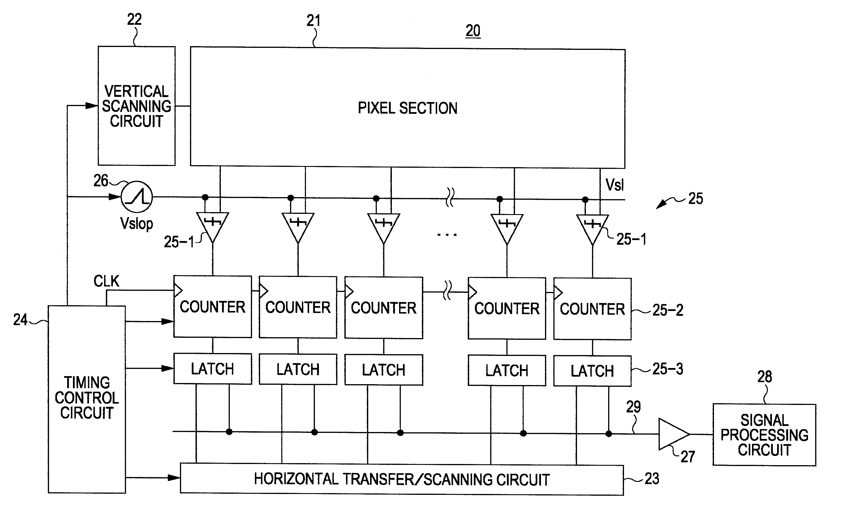
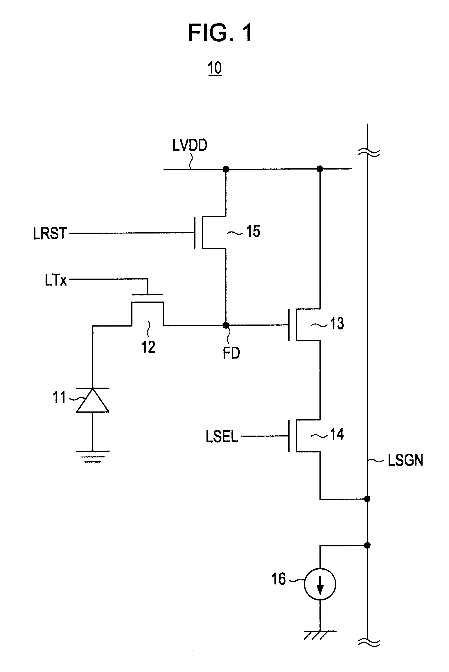
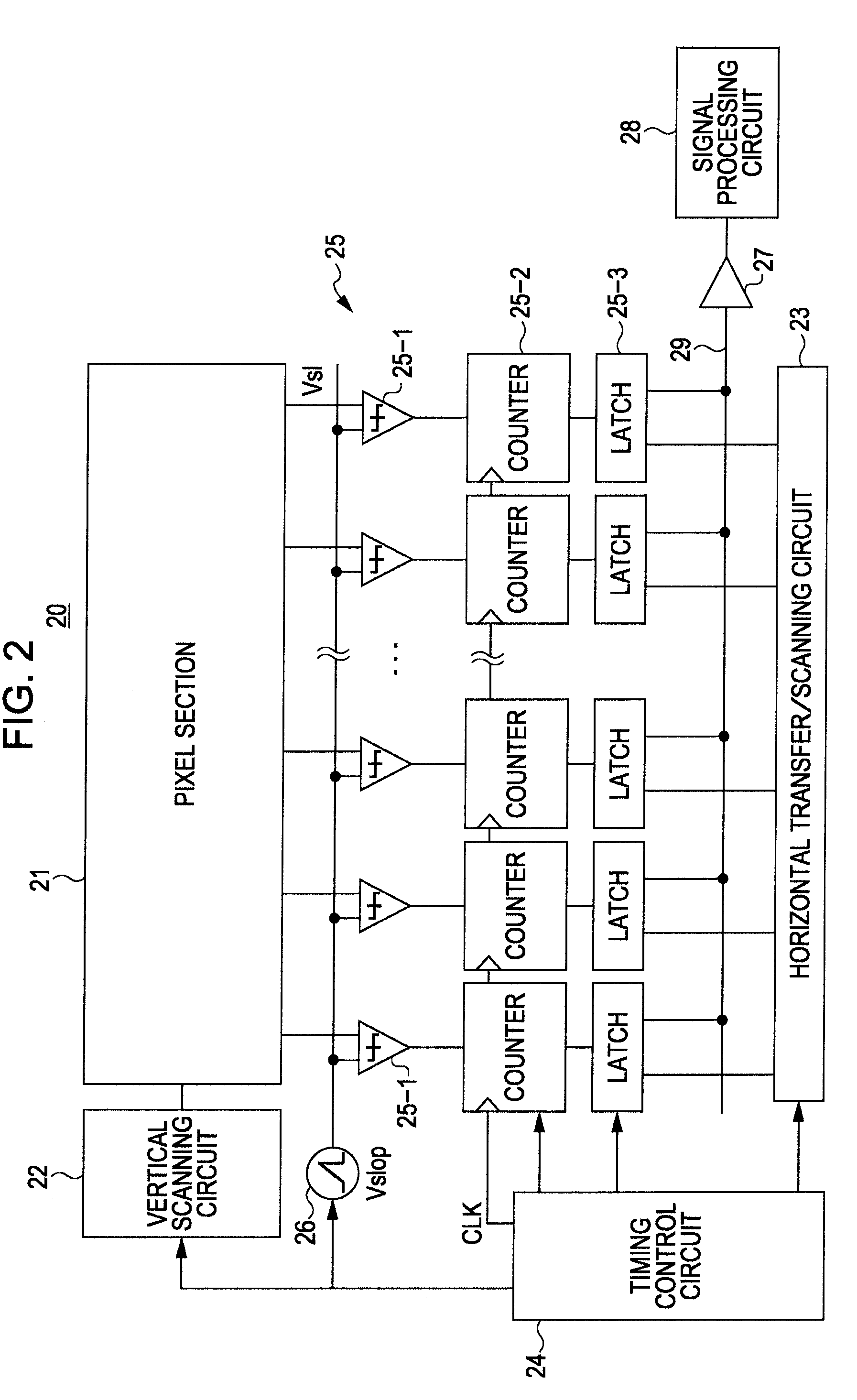
BACKGROUND OF THE INVENTION[0001]1. Field of the Invention[0002]The present invention relates to an analog-to-digital (AD) converter applicable to a solid-state image pickup device represented by, for example, a complementary metal-oxide semiconductor (CMOS) image sensor, an AD converting method, a solid-state image pickup device including the AD converter, and a camera system.[0003]2. Description of the Related Art[0004]In recent years, CMOS image sensors have been drawing attention as solid-state image pickup devices (image sensors), in place of charge-coupled device (CCD) image sensors.[0005]This is because CMOS image sensors overcome the problems of CCD image sensors, including that a dedicated manufacturing process is necessary for fabricating CCD pixels, a plurality of power supply voltages are necessary for the operation of a CCD image sensor, and a system including the CCD image sensor becomes very complicated due to the necessity of operating a plurality of peripheral integ...

Claims


Application Information

Patent Timeline
Patent Type & Authority Applications(United States)
IPC IPC(8): H04N5/335H03M1/34H03M1/10H03M1/14H03M1/18H03M1/56
CPCH04N5/355H04N5/3742H04N5/378H04N5/335H03M1/56H04N3/1512H04N3/155H03M1/18H04N25/00H04N25/57H04N25/616H04N25/767H04N25/76H04N25/75H04N23/00
Inventor OKUMURA, KENICHI
Owner SONY CORP
Why Eureka
Try Eureka