Semiconductor device and fabrication method thereof

a technology of semiconductor devices and semiconductor layers, applied in semiconductor devices, semiconductor/solid-state device details, electrical devices, etc., can solve problems such as severe deformation of circuitry formed on metal layers and reliability problems of metal layers

Active Publication Date: 2009-10-01
UTAC HEADQUARTERS PTE LTD
View PDF4 Cites 12 Cited by
  • Summary
  • Abstract
  • Description
  • Claims
  • Application Information

AI Technical Summary

Benefits of technology

[0017]Moreover, the present invention transforms the drawback of the conventional wet etching into the advantage of the present invention, i.e., using a thicker metal layer in performing the wet etching process so as to form the substrate having fine wires suitable for bonding with a flip-chip semiconductor chip and high reliability, thereby omitting the drawbacks of poor reliability caused by using thin metal layer in the wet etching process and avoiding increased costs and poor etching selectivity as encountered in the dry etching technique.
, i.e., using a thicker metal layer in performing the wet etching process so as to form the substrate having fine wires suitable for bonding with a flip-chip semiconductor chip and high reliability, thereby omitting the drawbacks of poor reliability caused by using thin metal layer in the wet etching process and avoiding increased costs and poor etching selectivity as encountered in the dry etching technique.

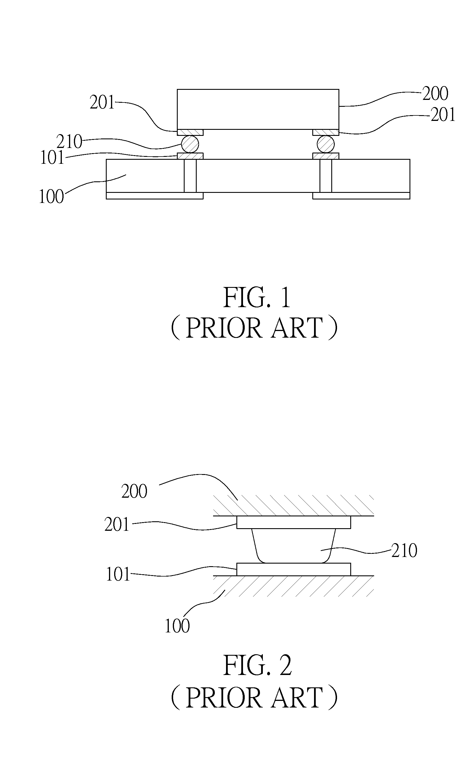
Problems solved by technology

The dry etching process ensures that the solder pad 101 has a precise size, but it is time-consuming.
However, with the wet etching process being an isotropic etching process and the metal layer being in contact with the etchant during the wet etching process, a circuitry formed on the metal layer is severely deformed.
The metal layer is confronted with a reliability problem such as the ease strip of the circuitry.

Method used


Image

  • Semiconductor device and fabrication method thereof
  • Semiconductor device and fabrication method thereof
  • Semiconductor device and fabrication method thereof

Examples


Embodiment Construction

[0022]The present invention is described in the following with specific embodiments, such that one skilled in the pertinent art can easily understand other advantages and effects of the present invention from the disclosure of the invention. The present invention may also be implemented and applied according to other embodiments, and the details may be modified based on different views and applications without departing from the spirit of the invention.

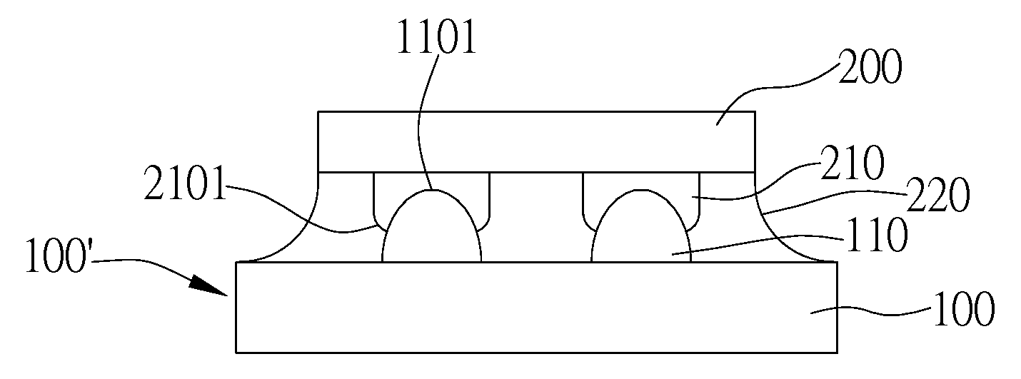
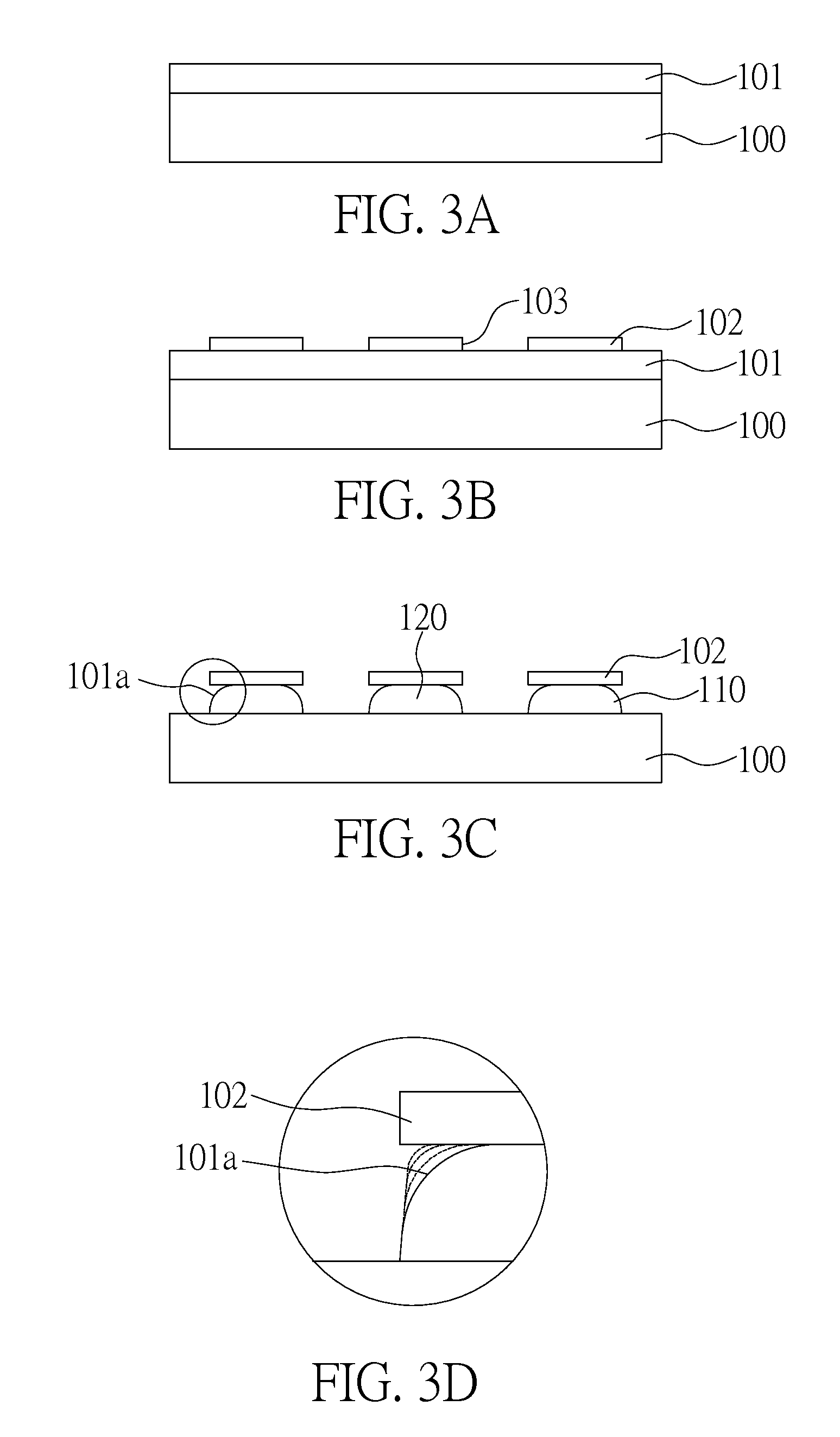
[0023]It should be understood that the fabrication method of the present invention includes providing a semiconductor chip having an inner circuit and a plurality of connection bumps electrically connected to the inner circuit, and a substrate having a plurality of solder pads formed by wet etching a conductive metal layer for being electrically connected to the connection bumps; flipping the semiconductor chip to make the connection bumps correspond to the solder pads in position; and compressing the substrate and the semiconductor c...


PUM


Abstract

A semiconductor device and a method of manufacturing the same are disclosed. The method is carried out by forming solder pads on a substrate by wet etching, flipping a semiconductor chip having a plurality of connection bumps formed on an active surface of the semiconductor chip for the connection bumps to be mounted by compression on the solder pads of the substrate correspondingly, at a temperature of the compression between the connection bumps and the solder pads lower than the melting points of the solder pads and the connection bumps, so as to allow the semiconductor chip to be engaged with and electrically connected to the substrate through the connection bumps and the solder pads, thereby enhancing the bonding strength of the solder pads and the connection bumps and increasing the fabrication reliability.

Description

FIELD OF THE INVENTION[0001]The present invention relates to semiconductor devices and fabrication methods thereof, and more particularly, to a flip-chip type of semiconductor device and a fabrication method thereof.BACKGROUND OF THE INVENTION[0002]Semiconductor devices have been applied to communication systems, networks, computers, electronic appliances, business machines, cameras, or even game machines. There is a great demand for semiconductor devices in various applications, such as industrial machines, peripheral tools and portable machines. With the rapid development of electronic industry, a semiconductor device is required to have a compact size, multiple pins and a low profile, without compromising functionalities and fabrication cost.[0003]In order to achieve the objectives of having a compact size, multiple pins and a low profile, a flip-chip type of semiconductor device, which is derived from a conventional wire bonding type of semiconductor device having gold wires to ...

Claims


Application Information

Patent Timeline
Patent Type & Authority Applications(United States)
IPC IPC(8): H01L23/485H01L21/50
CPCH01L24/16H01L2224/13099H01L2224/16H01L2924/01029H01L2924/01079H01L2924/01082H01L2224/814H01L2924/01006H01L2924/01033H01L2224/81193H01L2924/01005H01L2924/014H01L2924/351H01L2224/05573H01L2224/05568H01L2924/00014H01L2924/00H01L2224/05599
Inventor TSAI, SHIANN-TSONG
Owner UTAC HEADQUARTERS PTE LTD
Why Eureka
Try Eureka