Circuit Device

a circuit device and circuit technology, applied in the direction of semiconductor/solid-state device details, printed circuit non-printed electric components association, electrical apparatus construction details, etc., can solve the problems of photo couplers that cannot follow up electrical signals, photo couplers are difficult to be made smaller, and noise signals may be generated, so as to suppress the generation of noise signals and suppress the effect of noise signals

Inactive Publication Date: 2009-10-01
RENESAS ELECTRONICS CORP
View PDF7 Cites 40 Cited by
  • Summary
  • Abstract
  • Description
  • Claims
  • Application Information

AI Technical Summary

Benefits of technology

[0013]In the circuit device thus constructed, when an external magnetic field is applied to the circuit device, the first receiving inductor and the second receiving inductor generate a voltage in opposite directions. Also, the first receiving inductor and the second receiving inductor are connected in series. Accordingly, the output voltage of

Problems solved by technology

The photo coupler is, however, difficult to be made smaller because of including the light emitter and the photodetector.
Besides, in the case where the electrical signal has a high frequency, the photo coupler is unable to follow

Method used


Image

  • Circuit Device
  • Circuit Device
  • Circuit Device

Examples


first embodiment

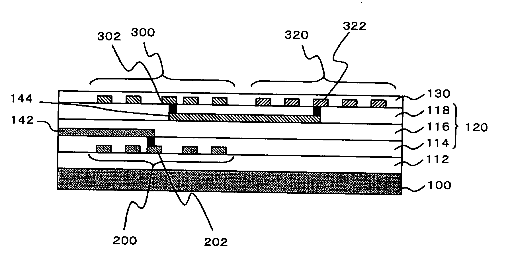
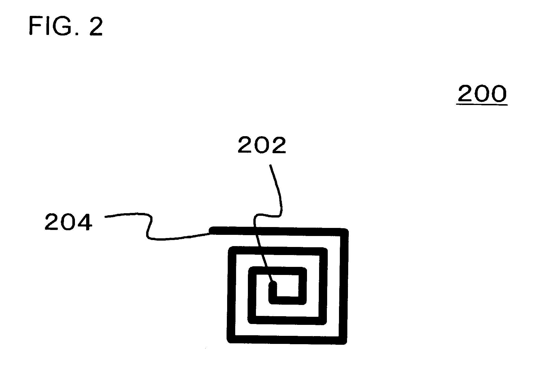
[0042]FIG. 1 is a cross-sectional view showing a circuit device according to a The circuit device includes a first transmitting inductor 200, a first insulating layer 120, a first receiving inductor 300, and a second receiving inductor 320. The first transmitting inductor 200 is constituted of a helical conductive pattern, and receives an input of a transmitted signal. The first insulating layer 120 is provided over or under the first transmitting inductor 200. In the example shown in FIG. 1, the first insulating layer 120 is located over the first transmitting inductor 200. The first receiving inductor 300 is located in a region overlapping with the first transmitting inductor 200 through the first insulating layer 120. The first receiving inductor 300 is constituted of a helical conductive pattern, and generates a received signal corresponding to the transmitted signal input to the first transmitting inductor 200. The second receiving inductor 320 is connected in series to the fi...

fifth embodiment

[0075]FIGS. 8A and 8B are plan views each showing a shape of an inductor of a circuit device according to a In this embodiment the circuit device includes an even number of signal transmitting circuits including the first transmitting inductor 200, the second transmitting inductor 220, the first receiving inductor 300, and the second receiving inductor 320. Each of the signal transmitting circuits is disposed such that the same inductors are located adjacent to each other. Between the signal transmitting circuits, no other inductor is provided.

[0076]FIG. 8A is a plan view showing the shape of the first transmitting inductor 200 and the second transmitting inductor 220. All the first transmitting inductors 200 and the second transmitting inductors 220 are connected in parallel to the first escape routing 142 serving as the input line of the transmitted signal, and to the interconnect 230. The first transmitting inductors 200 adjacently disposed generate a magnetic field in the oppos...

fourth embodiment

[0078]This embodiment also provides the same advantageous effects as those offered by the Also, the first transmitting inductors 200 adjacently disposed generate the magnetic field in the opposite directions upon receipt of the transmitted signal, and the second transmitting inductors 220 adjacently disposed also generate the magnetic field in the opposite directions. Accordingly, the magnetic fields generated by the adjacently disposed first transmitting inductors 200 are coupled with each other, and those generated by the adjacently disposed second transmitting inductors 220 are also coupled with each other. Such arrangement further minimizes the leakage of the magnetic field, thereby facilitating the first receiving inductor 300 and the second receiving inductor 320 to receive the signal.

[0079]FIG. 9 is a cross-sectional view showing a circuit device according to a sixth embodiment. This circuit device has the same structure as that of the first embodiment, except that a third r...


PUM


Abstract

The circuit device includes a first transmitting inductor, a first insulating layer, a first receiving inductor, and a second receiving inductor. The first transmitting inductor is constituted of a helical conductive pattern and receives a transmitted signal. The first receiving inductor is located in a region overlapping the first transmitting inductor through the first insulating layer. The first receiving inductor is constituted of a helical conductive pattern, and generates a received signal corresponding to the transmitted signal input to the first transmitting inductor. The second receiving inductor is connected in series to the first receiving inductor, and constituted of a helical conductive pattern. The second receiving inductor generates a voltage in an opposite direction to that generated by the first receiving inductor, in response to a magnetic field of the same direction.

Description

[0001]This application is based on Japanese patent application No. 2008-174111, the content of which is incorporated hereinto by reference.BACKGROUND[0002]1. Technical Field[0003]The present invention relates to a circuit device, capable of transmitting an electrical signal between two circuits unconnected to each other, and having high noise resistance.[0004]2. Related Art[0005]To transmit an electrical signal between two circuits that are different in potential of the electrical signal to be input, a photo coupler is generally employed. The photo coupler includes a light emitter such as a light emitting diode and a photodetector such as a photo transistor, and serves to convert the electrical signal that has been input into light with the light emitter, and restore the electrical signal from the light with the photodetector, to thereby transmit the electrical signal.[0006]The photo coupler is, however, difficult to be made smaller because of including the light emitter and the pho...

Claims


Application Information

Patent Timeline
IPC IPC(8): H05K1/16H01F5/00
CPCH01F17/0013H01F38/14H01F2017/0086H01F2038/143H01L2224/4813H01L2924/30107H01L2224/48137H01L2924/00H01L2924/00014H01F2017/0073H01L28/10H01L23/5227H01L2224/45099H01F27/2804H01F27/40H01F2027/2809H01L23/535H01L27/1203H01L29/0649
Inventor KAWANO, MASAYANAKASHIA, YASUTAKA
Owner RENESAS ELECTRONICS CORP
Why Eureka
Try Eureka