Silicon carbide semiconductor device comprising silicon carbide layer and method of manufacturing the same

a silicon carbide and semiconductor technology, applied in the direction of semiconductor devices, basic electric elements, electrical appliances, etc., can solve the problems of process failure in device manufacture, no detailed relation between the temperature of high-concentration ion implantation, and device manufacturing process failur

Active Publication Date: 2009-10-08
MITSUBISHI ELECTRIC CORP
View PDF9 Cites 27 Cited by
  • Summary
  • Abstract
  • Description
  • Claims
  • Application Information

AI Technical Summary

Benefits of technology

[0010]The present invention is made on the basis of recognition of the present circumstances, and it is an object of the present invention to establish a technique ...

Problems solved by technology

Since the crystal of the p++ layer is significantly degraded when implantation of such high-concentration ions is performed at room temperature, this causes a process failure in manufacture of devices.
In well-known te...

Method used


Image

  • Silicon carbide semiconductor device comprising silicon carbide layer and method of manufacturing the same
  • Silicon carbide semiconductor device comprising silicon carbide layer and method of manufacturing the same
  • Silicon carbide semiconductor device comprising silicon carbide layer and method of manufacturing the same

Examples


Embodiment Construction

The First Preferred Embodiment

[0041]Detailed discussion will be made below on the effect of a high temperature process on a p++ region for silicon carbide p-type base ohmic contact which is manufactured by a method of manufacturing a silicon carbide semiconductor device in accordance with the first preferred embodiment.

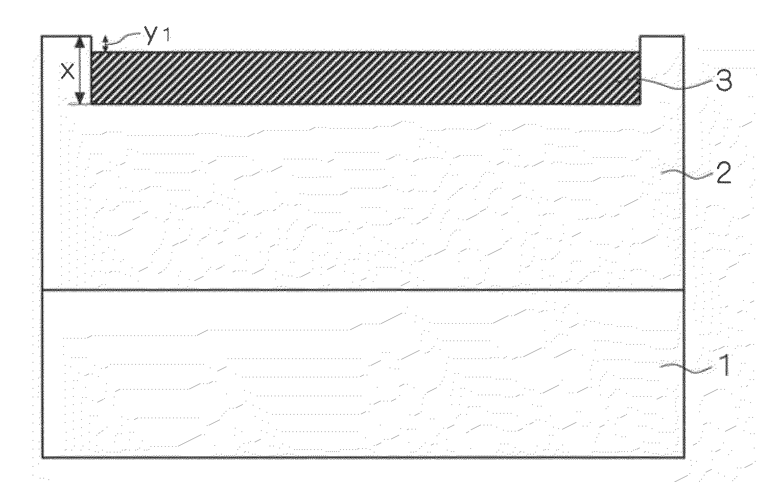
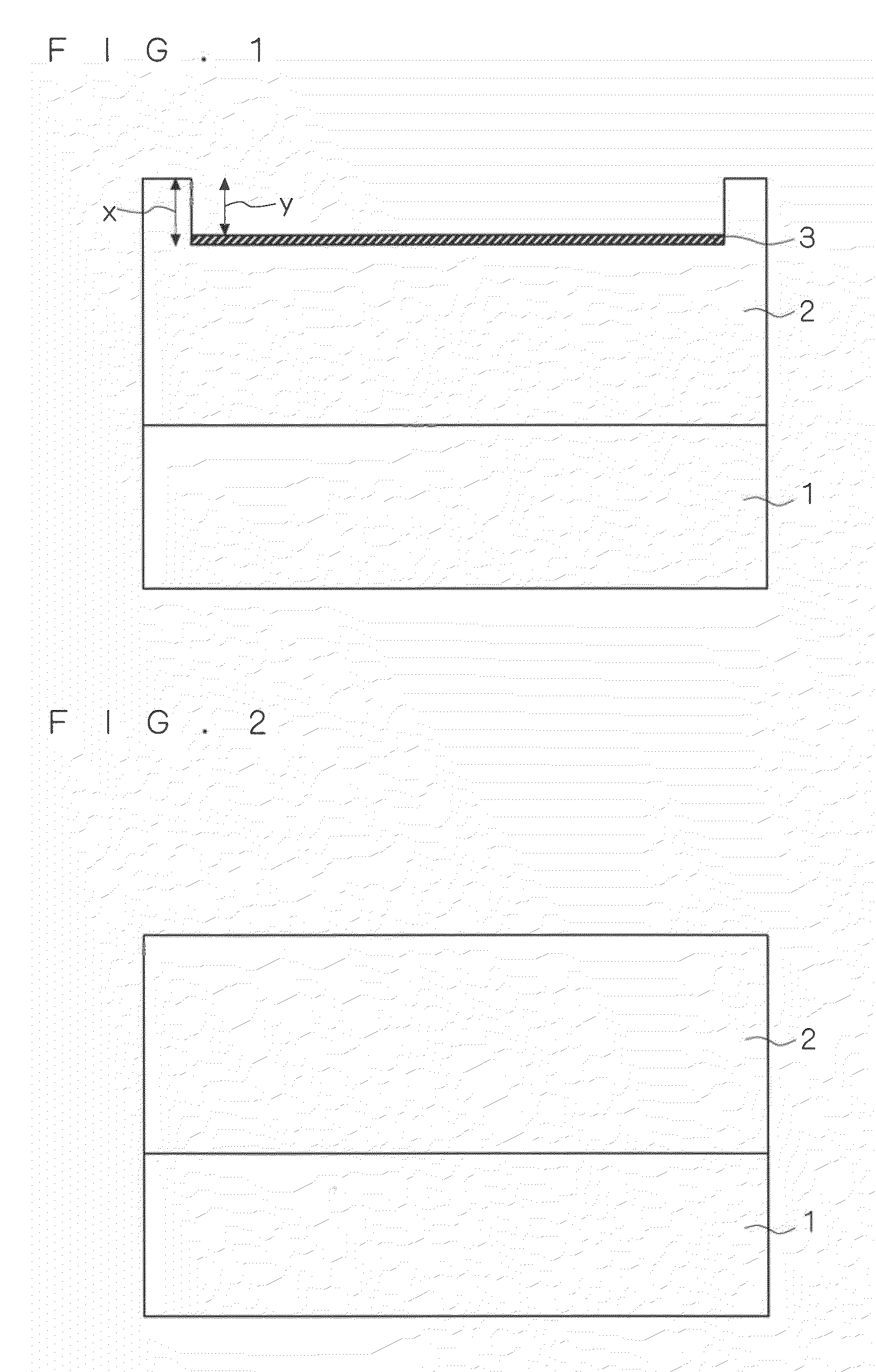
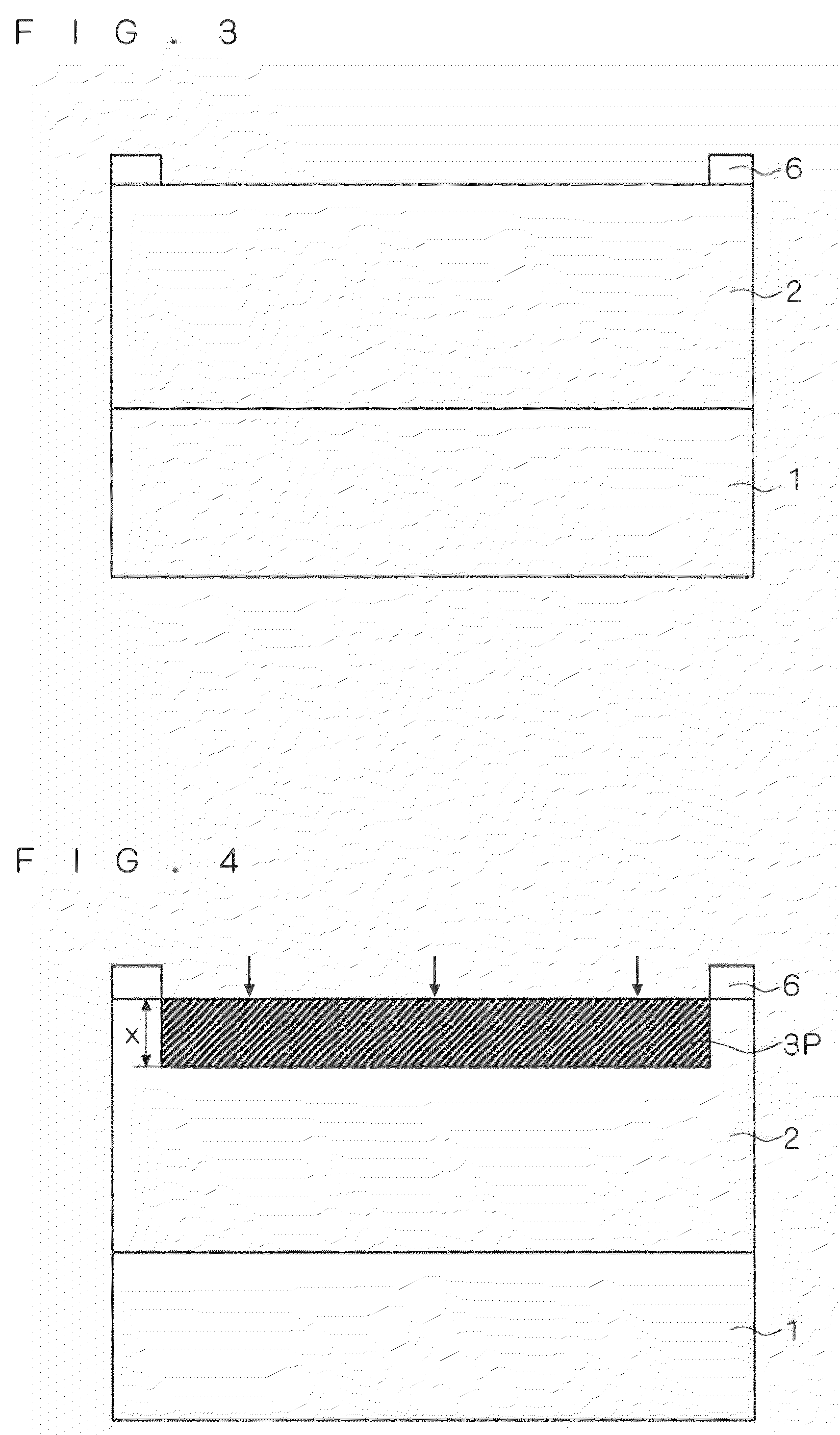
[0042]FIG. 1 is a longitudinal section showing a structure of a semiconductor device used to evaluate the effect of a process on the p++ region for silicon carbide p-type base ohmic contact. In FIG. 1, reference numeral 1 represents a silicon carbide substrate, reference numeral 2 represents a silicon carbide epitaxial layer grown on a surface of the silicon carbide substrate 1 and reference numeral 3 represents a p++ region formed on a surface of a step groove of the silicon carbide epitaxial layer 2.

[0043]Next, a procedure for evaluating the effect of a process on the p++ region for silicon carbide p-type base ohmic contact 3 in the first preferred embodiment will b...


PUM


Abstract

A p base ohmic contact of a silicon carbide semiconductor device consists of a p++ layer formed by high-concentration ion implantation and a metal electrode. Since the high-concentration ion implantation performed at the room temperature significantly degrades the crystal of the p++ layer to cause a process failure, a method for implantation at high temperatures is used. In terms of switching loss and the like of devices, it is desirable that the resistivity of the p base ohmic contact should be lower. In well-known techniques, nothing is mentioned on a detailed relation among the ion implantation temperature, the ohmic contact resistivity and the process failure. Then, in the ion implantation step, the temperature of a silicon carbide wafer is maintained in a range from 175° C. to 300° C., more preferably in a range from 175° C. to 200° C. The resistivity of the p base ohmic contact using a p++ region formed by ion implantation at a temperature in a range from 175° C. to 300° C. becomes lower than that in a case where the p++ region is formed by ion implantation at a temperature over 300° C. Further, this can avoid any process failure.

Description

BACKGROUND OF THE INVENTION[0001]1. Field of the Invention[0002]The present invention relates to a technique for manufacturing a silicon carbide semiconductor device.[0003]2. Description of the Background Art[0004]In order to break the limitation of properties of power devices using silicon, development of power devices using silicon carbide has been made. Especially, p-type ohmic contact of low resistivity is an essential element for a silicon carbide semiconductor device and in order to achieve it, it is very important to establish a technique for forming a high-concentration p++ layer.[0005]In a method of forming a p-type base ohmic contact shown in Japanese Patent Application Laid Open Gazette No. 2007-66959 (Patent Document 1), for forming a p++ layer for contact, ion implantation (Al, B, Ga) is performed under an atmosphere of the temperature of 400° C. or higher and this makes it possible to avoid any process failure occurring in manufacture of silicon carbide MOSFETs.[0006]F...

Claims


Application Information

Patent Timeline
IPC IPC(8): H01L29/24H01L21/34
CPCH01L21/046H01L21/0485H01L29/7828H01L29/66068H01L29/7802H01L29/1608
Inventor WATANABE, TOMOKATSUAYA, SUNAOMIURA, NARUHISASAKAI, KEIKOYOSHIDA, SHOHEITANIOKA, TOSHIKAZUNAKAO, YUKIYASUTARUI, YOICHIROIMAIZUMI, MASAYUKI
Owner MITSUBISHI ELECTRIC CORP
Why Eureka
Try Eureka