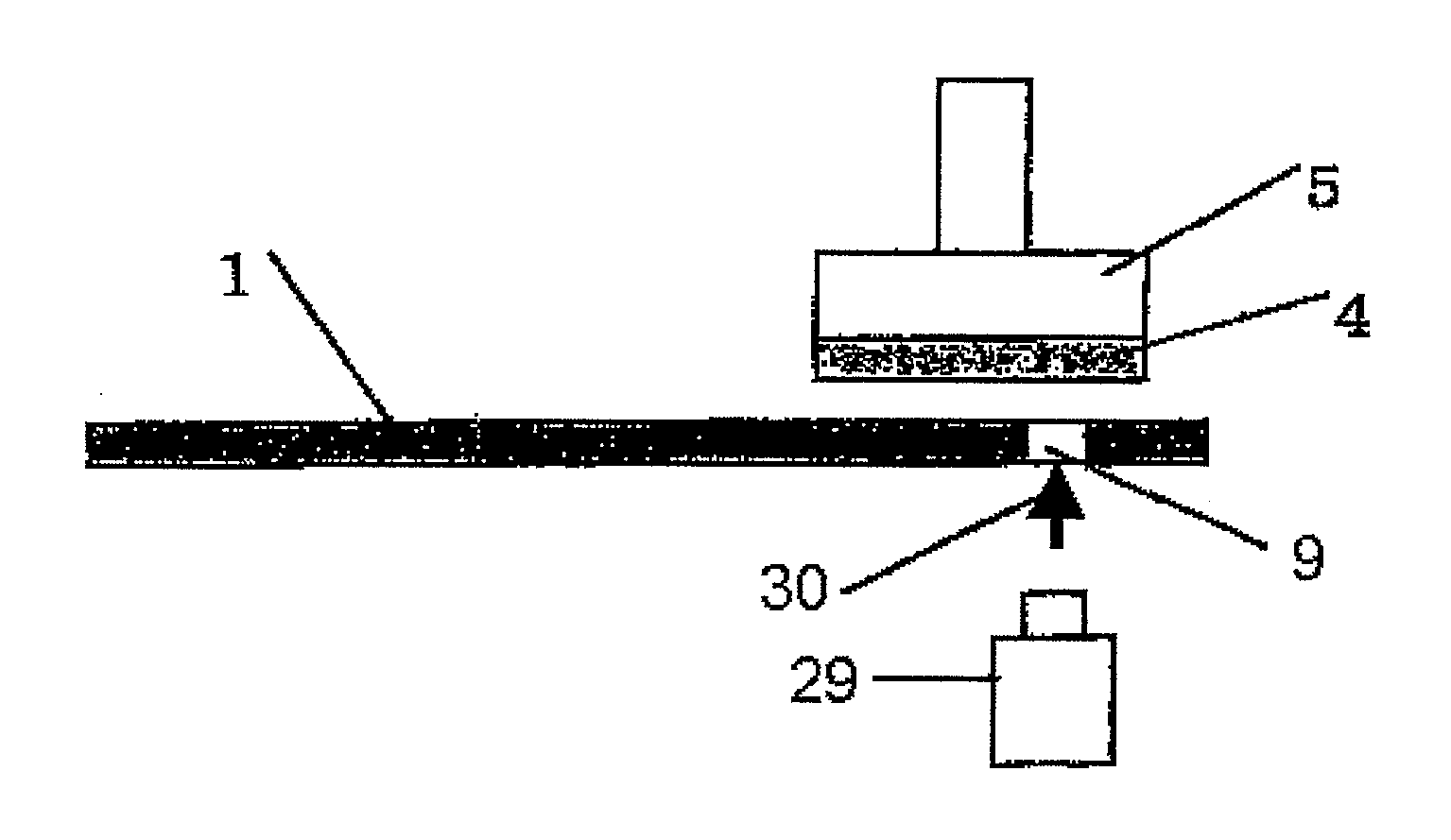
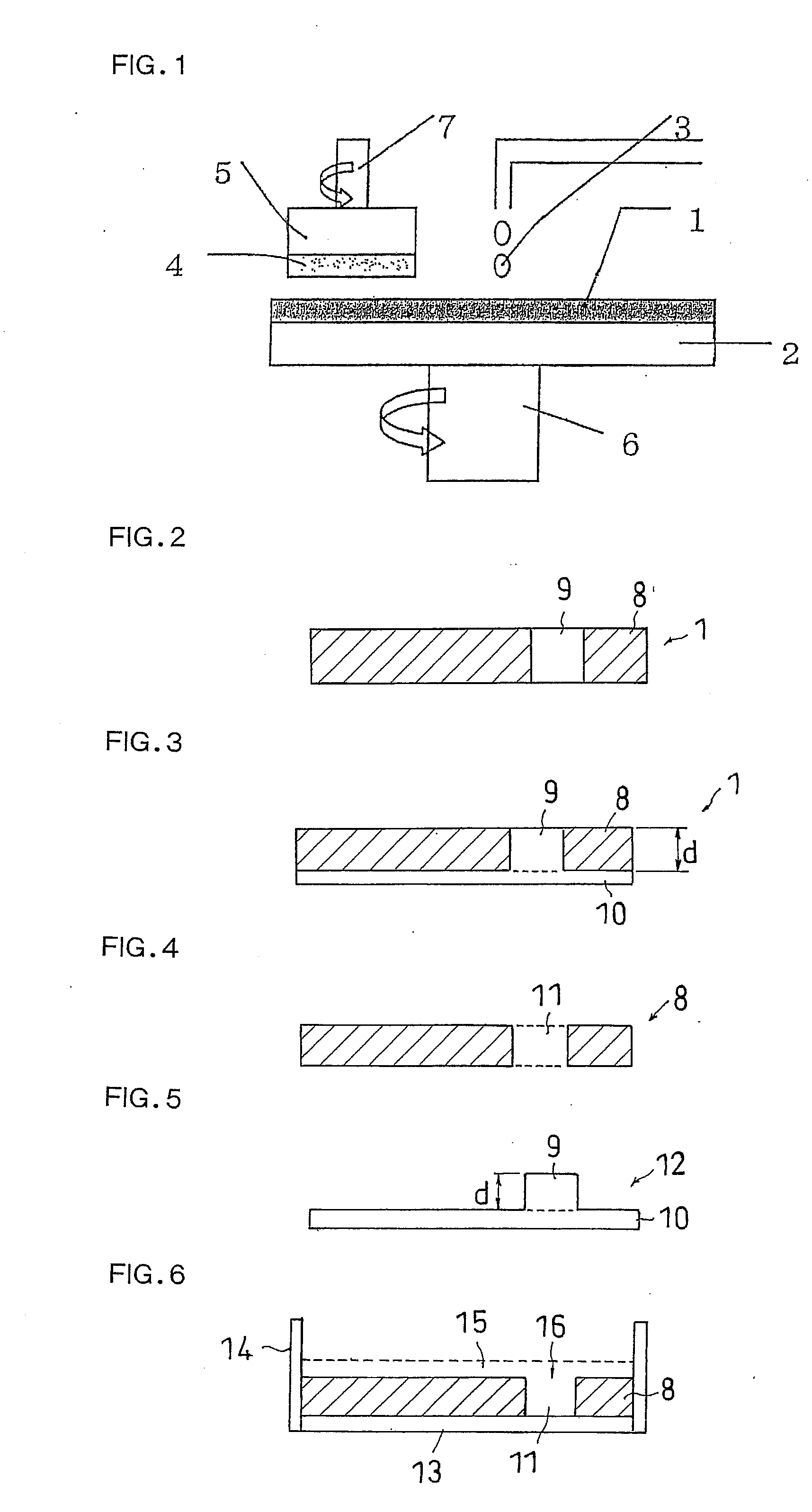
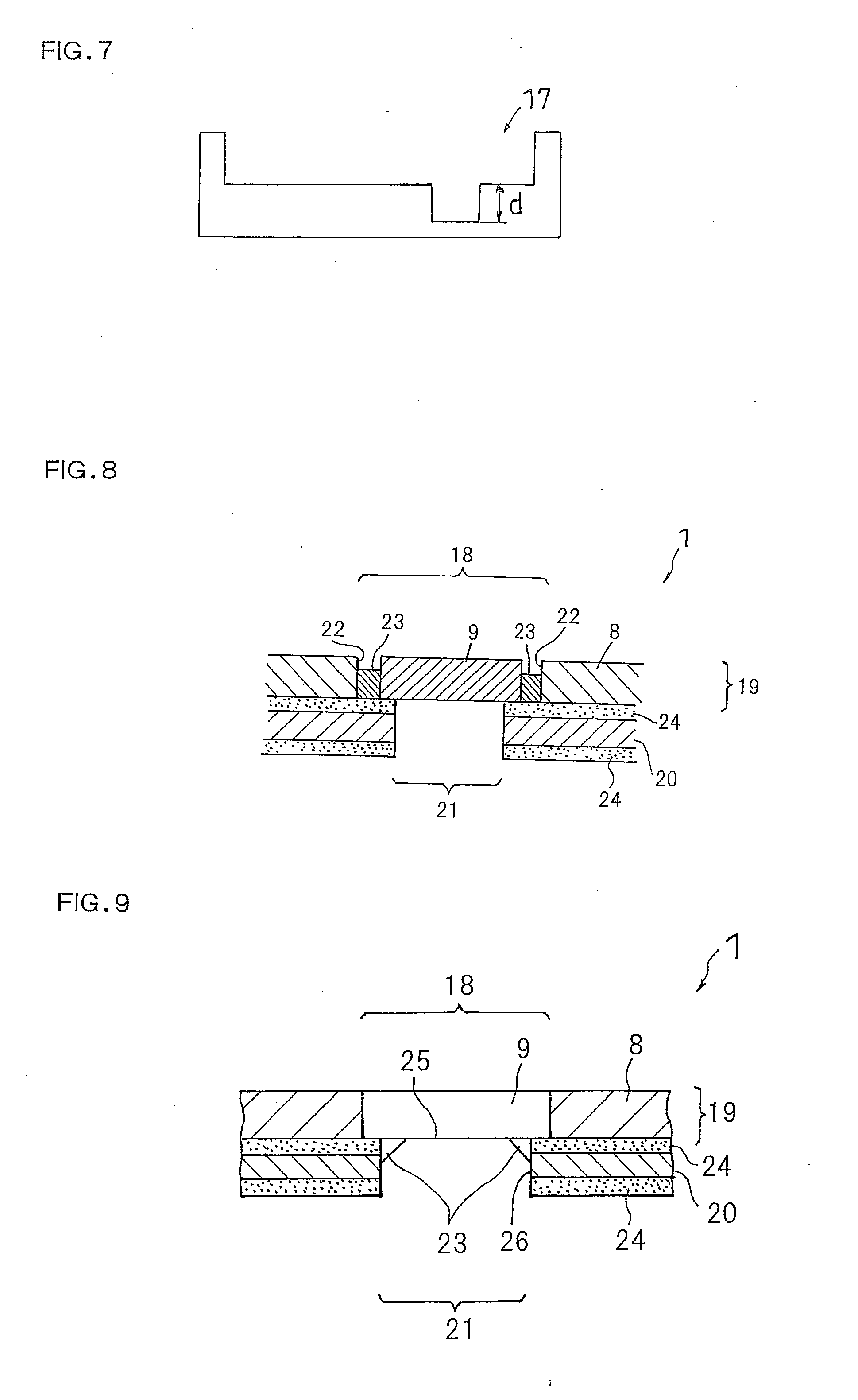
Polishing pad

a technology of polishing pad and slurry, which is applied in the field of polishing pad, can solve the problems of reducing the detection precision of an endpoint or disabling detection, and achieve the effects of suppressing the deterioration of polishing characteristics, high-precision optical detection, and preventing slurry leakag

Active Publication Date: 2009-10-08
ROHM & HAAS ELECTRONICS MATERIALS CMP HLDG INC
View PDF10 Cites 79 Cited by
  • Summary
  • Abstract
  • Description
  • Claims
  • Application Information

AI Technical Summary

Benefits of technology

[0020]The invention has been made in order to solve the above problem and it is an object of the invention to provide a polishing pad capable of high precision optical detection of an endpoint during polishing in progress and prevention of slurry leakage from between a polishing region and a light-transmitting region during the use thereof even after the polishing pad has been used for a long period. It is a second object of the invention to provide a polishing pad capable of suppression of deterioration of polishing characteristics (such as in-plane uniformity) and generation of scratches due to a difference in behavior of a polishing region and a light-transmitting region during polishing. It is a third object of the invention to provide a polishing pad having a polishing region and a light-transmitting region with a concentration of a specific metal equal to or lower than a specific value (threshold value). It is a fourth object of the invention to provide a method for fabricating a semiconductor device using the polishing pad.

Problems solved by technology

The slurry leakage is thought to cause optical problems such as a clouding on a light detector, thereby reducing a detection precision of an endpoint or disabling the detection thereof.

Method used


Image

  • Polishing pad
  • Polishing pad
  • Polishing pad

Examples


example 6

[0300]A polishing pad was manufactured by means of a similar method to that in Example 2 with the exception that, in Example 2, 80 parts by wt of liquid urethane acrylate (Actilane 290, manufactured by Aczo Nobeles Co.), 20 parts by wt of liquid urethane acrylate (UA-101H, manufactured by Kyoeisha Chemical Co., Ltd.) were used instead of 100 parts by wt of liquid urethane acrylate (Actilane 290, manufactured by AKCROS CHEMICALS CO.). A light-transmitting region has physical properties of an Asker hardness A of 87 degrees, a compressibility of 1.3% and a compression recovery percentage of 94.3%.

example 7

[0301]A polishing pad was manufactured by means of a similar method to that in Example 3 with the exception that, in Example 3, 80 parts by wt of liquid urethane acrylate (Actilane 290, manufactured by Aczo Nobeles Co.), 20 parts by wt of liquid urethane acrylate (UA-101H, manufactured by Kyoeisha Chemical Co., Ltd.) were used instead of 100 parts by wt of liquid urethane acrylate (Actilane 290, manufactured by AKCROS CHEMICALS CO.). A light-transmitting region has physical properties of an Asker hardness A of 87 degrees, a compressibility of 1.3% and a compression recovery percentage of 94.3%.

example 8

[0302]A polishing pad was manufactured by means of a similar method to that in Example 4 with the exception that, in Example 4, 80 parts by wt of liquid urethane acrylate (Actilane 290, manufactured by Aczo Nobeles Co.), 20 parts by wt of liquid urethane acrylate (UA-101H, manufactured by Kyoeisha Chemical Co., Ltd.) were used instead of 100 parts by wt of liquid urethane acrylate (Actilane 290, manufactured by AKCROS CHEMICALS CO.). A light-transmitting region has physical properties of an Asker hardness A of 87 degrees, a compressibility of 1.3% and a compression recovery percentage of 94.3%. The foam layer has physical properties of an Asker hardness A of 80 degrees, a compressibility of 3.4% and a compression recovery percentage of 93.1%.


PUM

PropertyMeasurementUnit
light transmittanceaaaaaaaaaa
wavelengthaaaaaaaaaa

Abstract

It is an object of the invention to provide a polishing pad capable of high precision optical detection of an endpoint during polishing in progress and prevention of slurry leakage from between a polishing region and a light-transmitting region during the use thereof even after the polishing pad has been used for a long period. It is a second object of the invention to provide a polishing pad capable of suppression of deterioration of polishing characteristics (such as in-plane uniformity) and generation of scratches due to a difference in behavior of a polishing region and a light-transmitting region during polishing. It is a third object of the invention to provide a polishing pad having a polishing region and a light-transmitting region with a concentration of a specific metal equal to or lower than a specific value (threshold value).

Description

TECHNICAL FIELD[0001]The present invention relates to a polishing pad used in planarizing an uneven surface of a wafer by chemical mechanical polishing (CMP) and in particular to a polishing pad having a window for sensing a polished state etc. by an optical means, as well as a method of producing a semiconductor device by the polishing pad.BACKGROUND ART[0002]Production of a semiconductor device involves a step of forming an electroconductive film on the surface of a wafer to form a wiring layer by photolithography, etching etc., a step of forming an interlaminar insulating film on the wiring layer, etc., and an uneven surface made of an electroconductive material such as metal and an insulating material is generated on the surface of a wafer by these steps. In recent years, processing for fine wiring and multilayer wiring is advancing for the purpose of higher integration of semiconductor integrated circuits, and accordingly techniques of planarizing an uneven surface of a wafer h...

Claims


Application Information

Patent Timeline
Patent Type & Authority Applications(United States)
IPC IPC(8): B24B37/04B24B1/00B29C65/70B32B37/00B32B3/10B24B37/20
CPCB24B37/205Y10T428/24339Y10T428/24992B24B37/24B24B37/26H01L21/304
Inventor OGAWA, KAZUYUKISHIMOMURA, TETSUOKAZUNO, ATSUSHINAKAI, YOSHIYUKIWATANABE, MASAHIROYAMADA, TAKATOSHINAKAMORI, MASAHIKO
Owner ROHM & HAAS ELECTRONICS MATERIALS CMP HLDG INC
Why Eureka
Try Eureka