

Semiconductor device and method for manufacturing the same
a semiconductor compound and semiconductor technology, applied in the direction of semiconductor devices, transistors, electrical devices, etc., can solve the problems of forming defects in devices, reducing the efficiency of semiconductor devices,
- Summary
- Abstract
- Description
- Claims
- Application Information
AI Technical Summary
Benefits of technology
Problems solved by technology
Method used
Image

Examples
Embodiment Construction
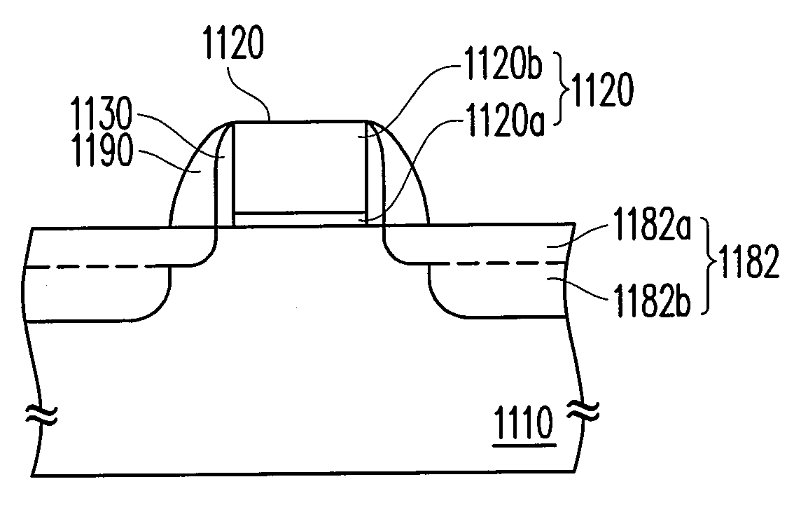
[0040]In the present invention, a solid-phase epitaxy (SPE) process is utilized to form a semiconductor compound solid-phase epitaxy layer having a strain (tensile stress or compression stress) so as to achieve strain control. The SPE process includes a first strain atom implantation and a second strain atom implantation with energies different from each other so as to form strain regions at two sides of a gate structure in a substrate. Afterwards, a solid-phase epitaxy annealing process is performed so that the strain atoms in the strain regions epitaxy grow into a semiconductor compound solid-phase epitaxy layer.
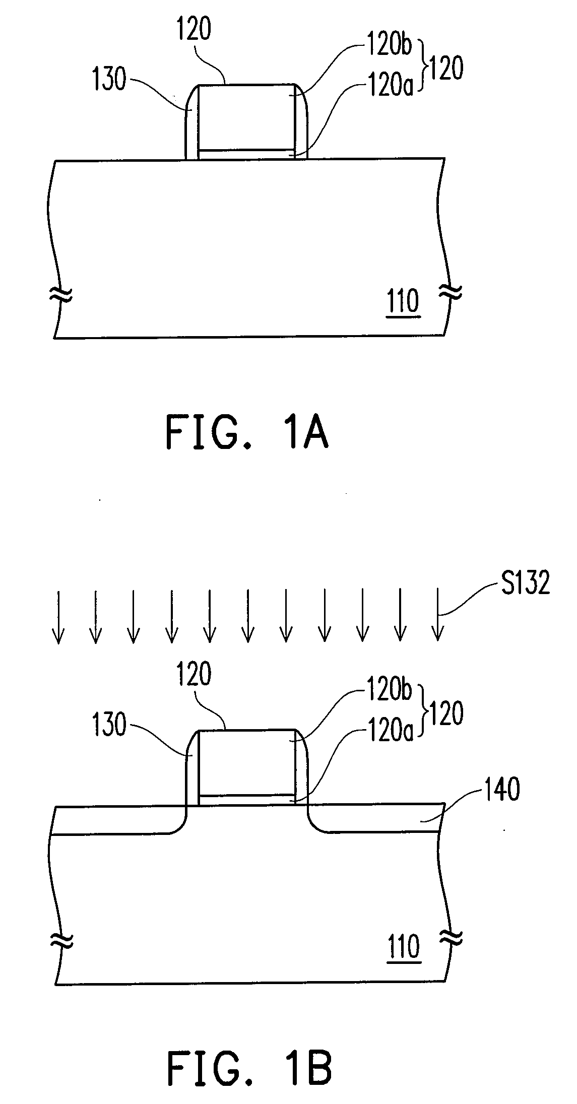
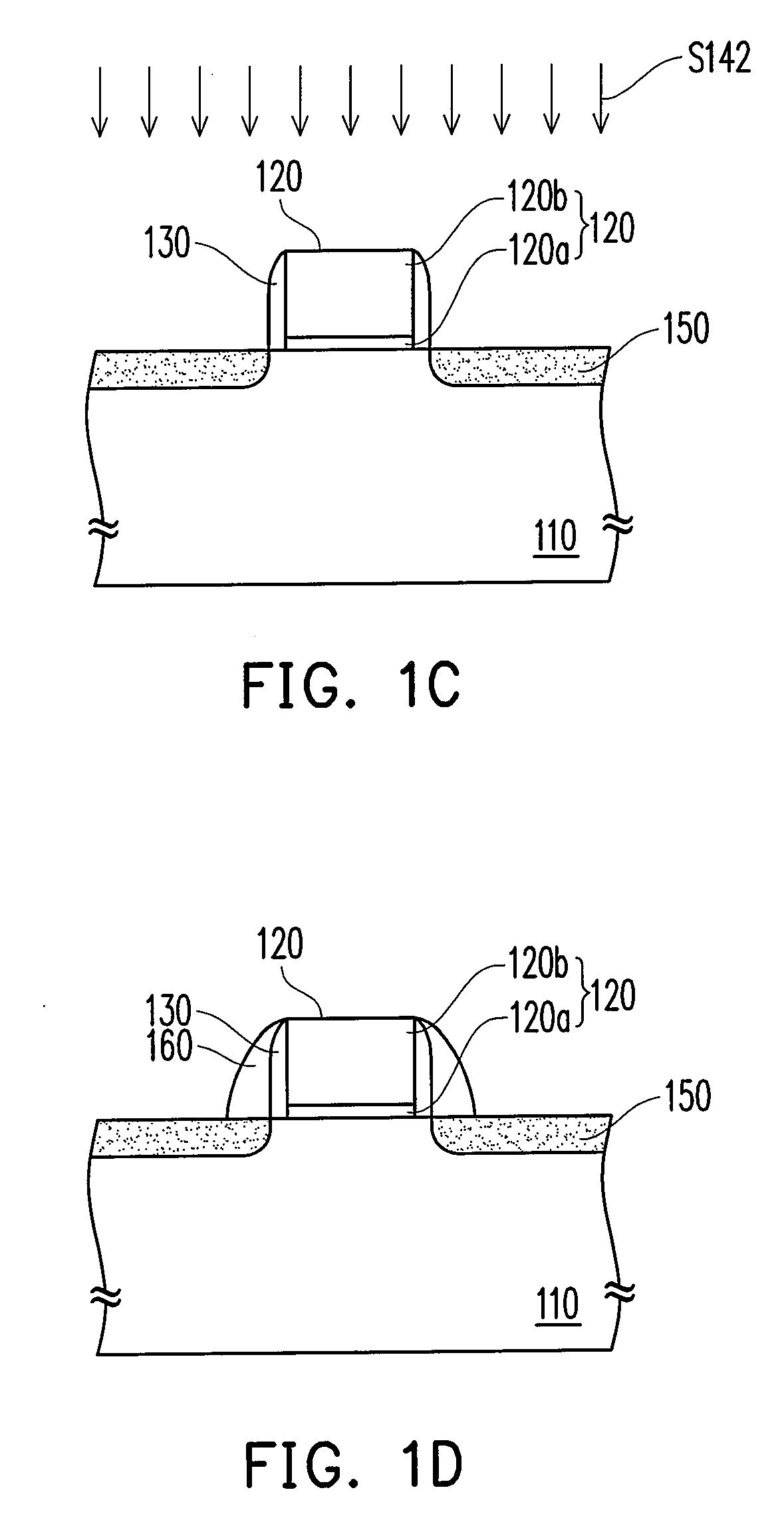
[0041]FIG. 1 is a flowchart of manufacturing a semiconductor device according to the first embodiment of the present invention. FIGS. 1A through 1G are schematic cross-sectional views illustrating a process flow of manufacturing a semiconductor device according to the first embodiment of the present invention.
[0042]First, referring to FIGS. 1 and 1A, a step S120 is perform...
PUM
 Abstract
Description
Claims
Application Information