Device and process for applying and/or detaching a wafer to/from a carrier
- Summary
- Abstract
- Description
- Claims
- Application Information
AI Technical Summary
Benefits of technology
Problems solved by technology
Method used
Image
Examples
Embodiment Construction
[0055]In the figures, the same components and the components with the same function are identified with the same reference numbers.
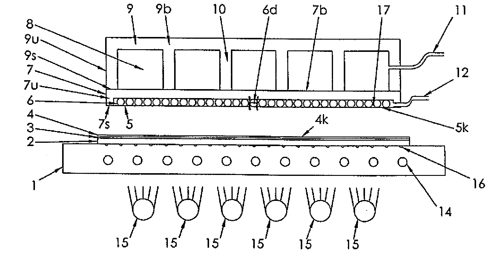
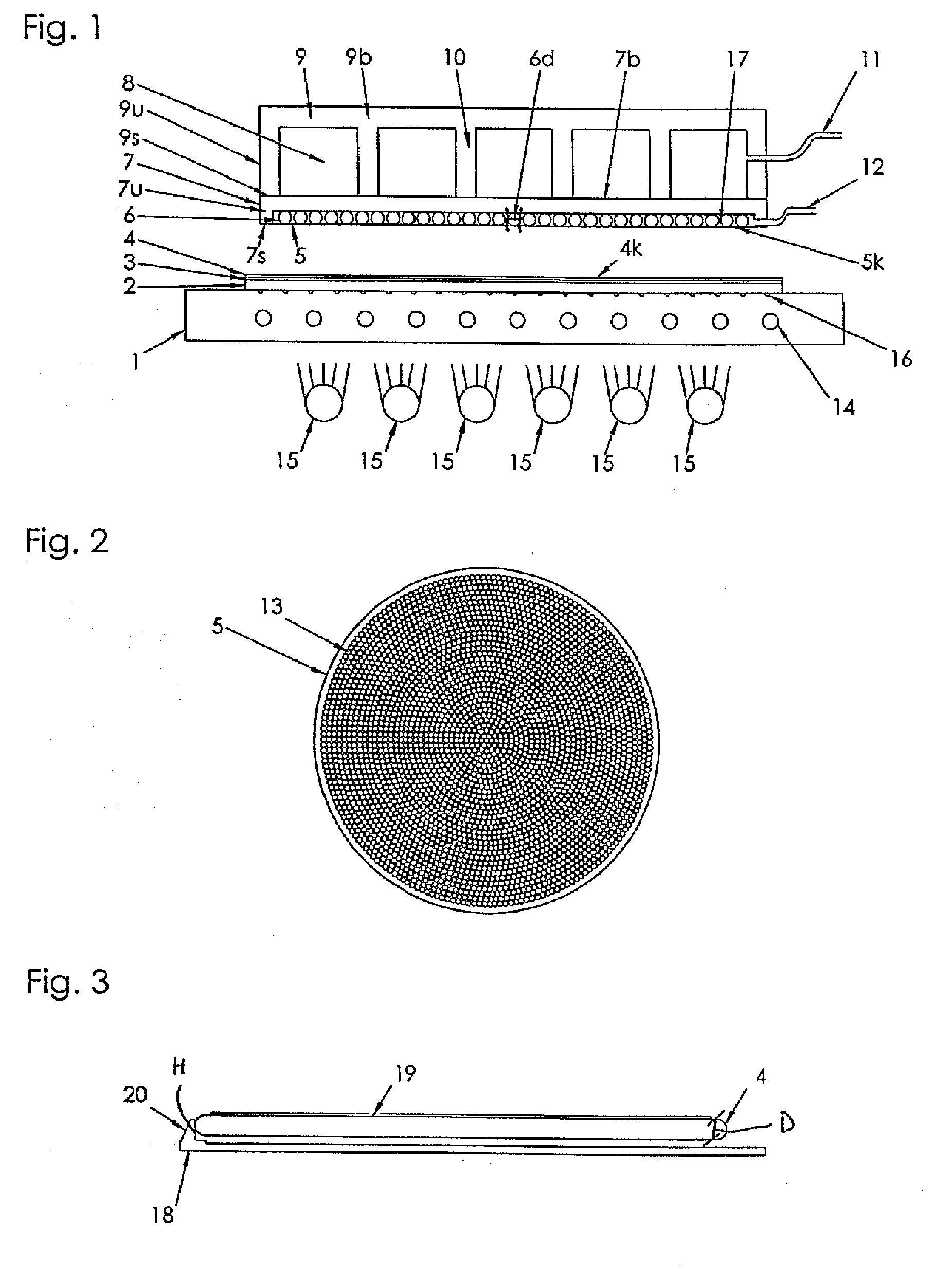
[0056]FIG. 1 schematically shows a device as claimed in the invention as an embodiment, components such as the housing which surrounds the device or positioning and / or adjusting means, such as for example a robot arm, not being shown, since they are relatively known in the prior art.
[0057]A carrier 2 can be fixed by negative pressure fixing means 16 on a receiving unit 1 with the heating means 14 which are integrated into it and which are made here as heating coils. A wafer 4 is joined to the carrier 2 by connecting means 3, for example a cement, and the wafer has been re-thinned in a previous process step so that one contact surface 4k of the wafer 4 on the side of the wafer 4 facing away from the carrier 2 is exposed.
[0058]An important component of the device as claimed in the invention is the means consisting of the components located above the wafer ...
PUM
| Property | Measurement | Unit |
|---|---|---|
| Pressure | aaaaa | aaaaa |
| Diameter | aaaaa | aaaaa |
| Adhesion strength | aaaaa | aaaaa |
Abstract
Description
Claims
Application Information

