Liquid crystal display and electronic apparatus

a technology of electronic equipment and liquid crystal display, which is applied in the direction of instruments, non-linear optics, optics, etc., can solve the problems of narrow viewing angle, unclear image with contrast, and light leakage from the region, and achieve the effect of high contrast ratio

Inactive Publication Date: 2009-10-22
JAPAN DISPLAY WEST
View PDF9 Cites 18 Cited by
  • Summary
  • Abstract
  • Description
  • Claims
  • Application Information

AI Technical Summary

Benefits of technology

[0023]With this configuration, it is possible to provide an electronic apparatus inclu

Problems solved by technology

As a result, the viewing angle becomes narrow.
When this happens, light leakage occurs from the region where the slope portion is formed.
Light leakage causes an unclear image with contrast deteriorated.
In this case, however, the pixel aperture ratio decreases so much.
In the case of a high-definition pixel, luminance is deteriorated, and a satisfactory display characteristic is not attained.
The slope portion may cause a difference in optical path of light transmitting the liquid crystal layer, and consequently a phase difference.
However, similarly to the abov

Method used


Image

  • Liquid crystal display and electronic apparatus
  • Liquid crystal display and electronic apparatus
  • Liquid crystal display and electronic apparatus

Examples


first embodiment

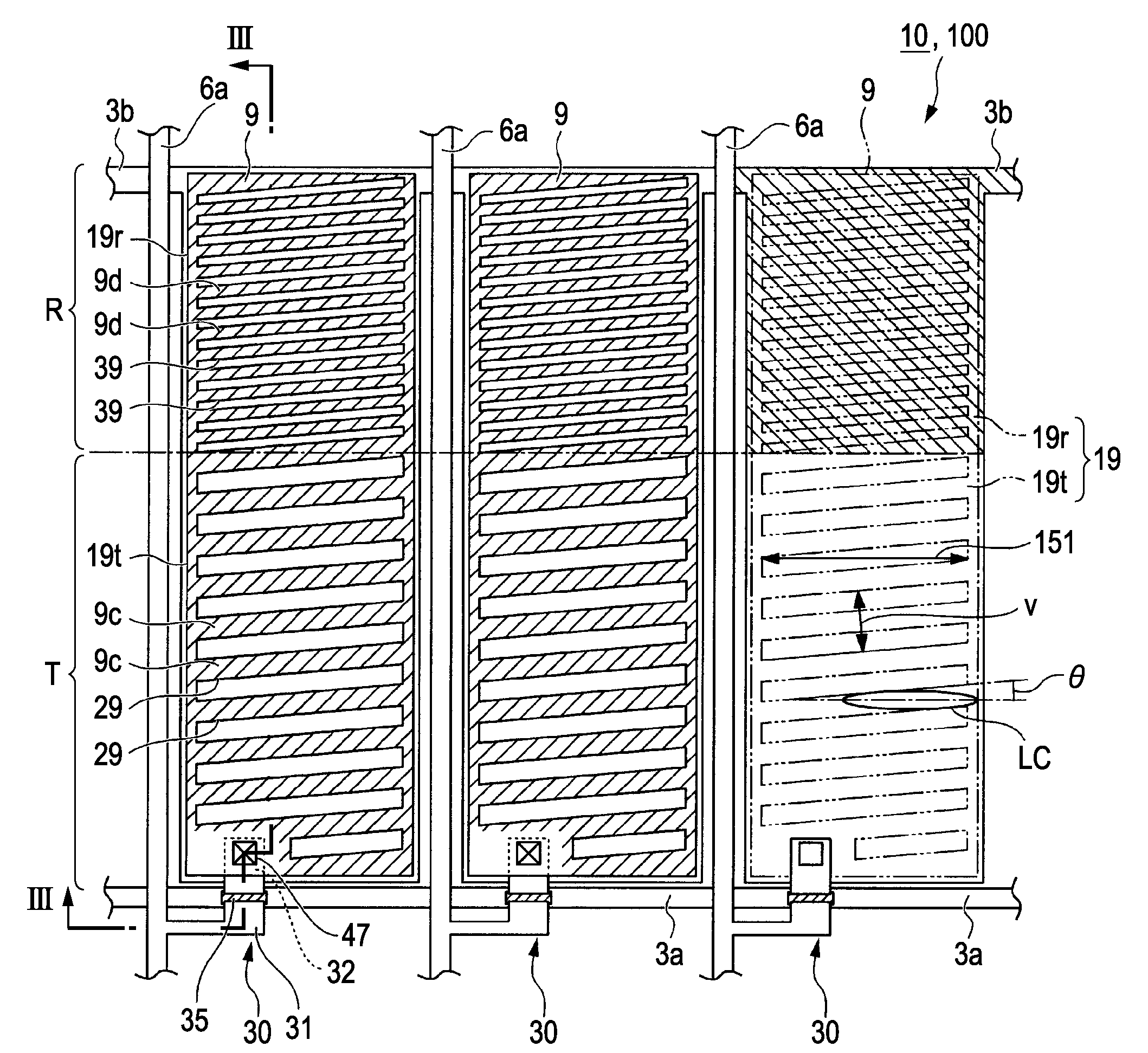
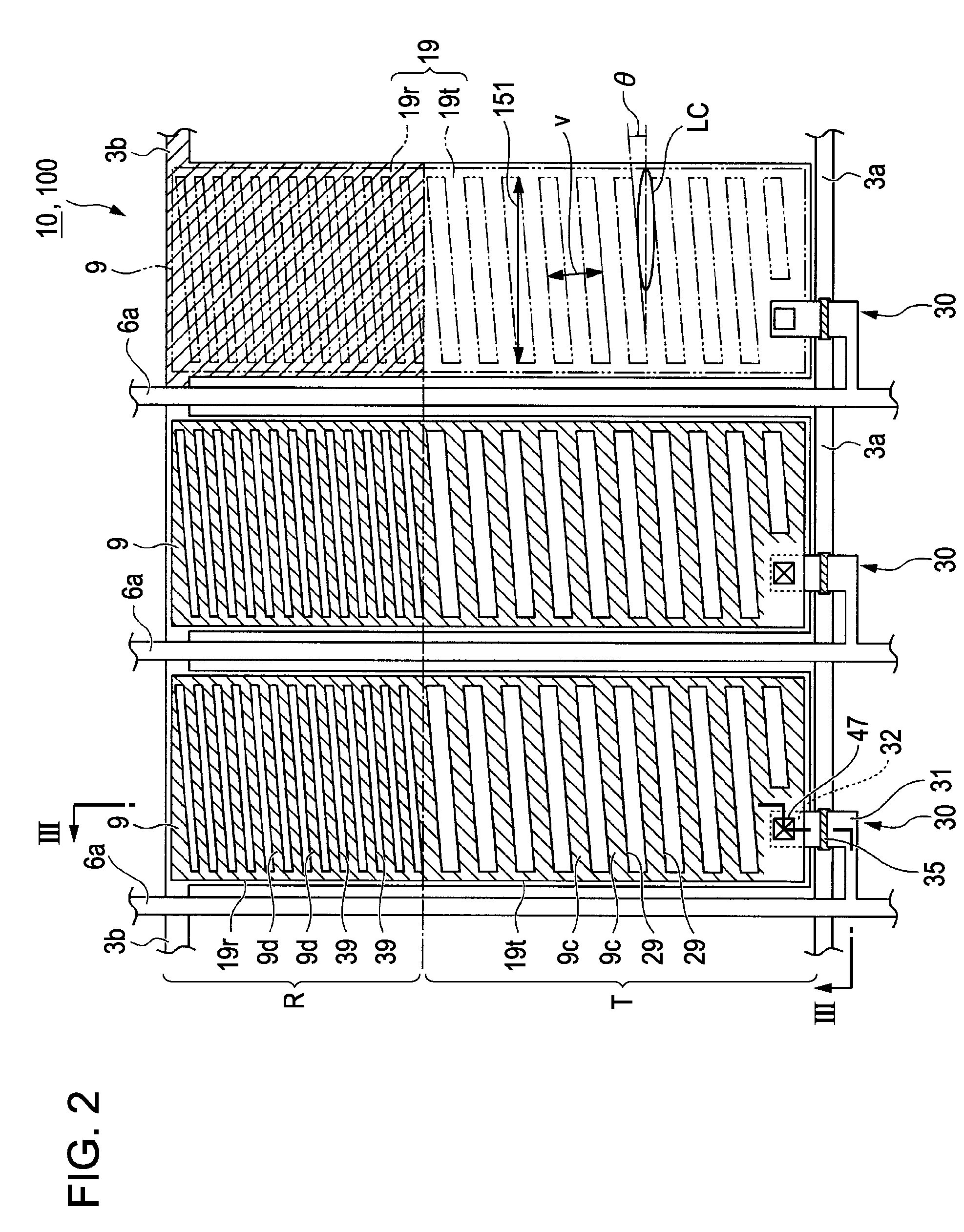
[0032]Hereinafter, a liquid crystal display according to a first embodiment of the invention will be described with reference to FIGS. 1 to 5B. In the drawings, the scale of thickness or dimension of each constituent element has been adjusted so as to be recognizable.

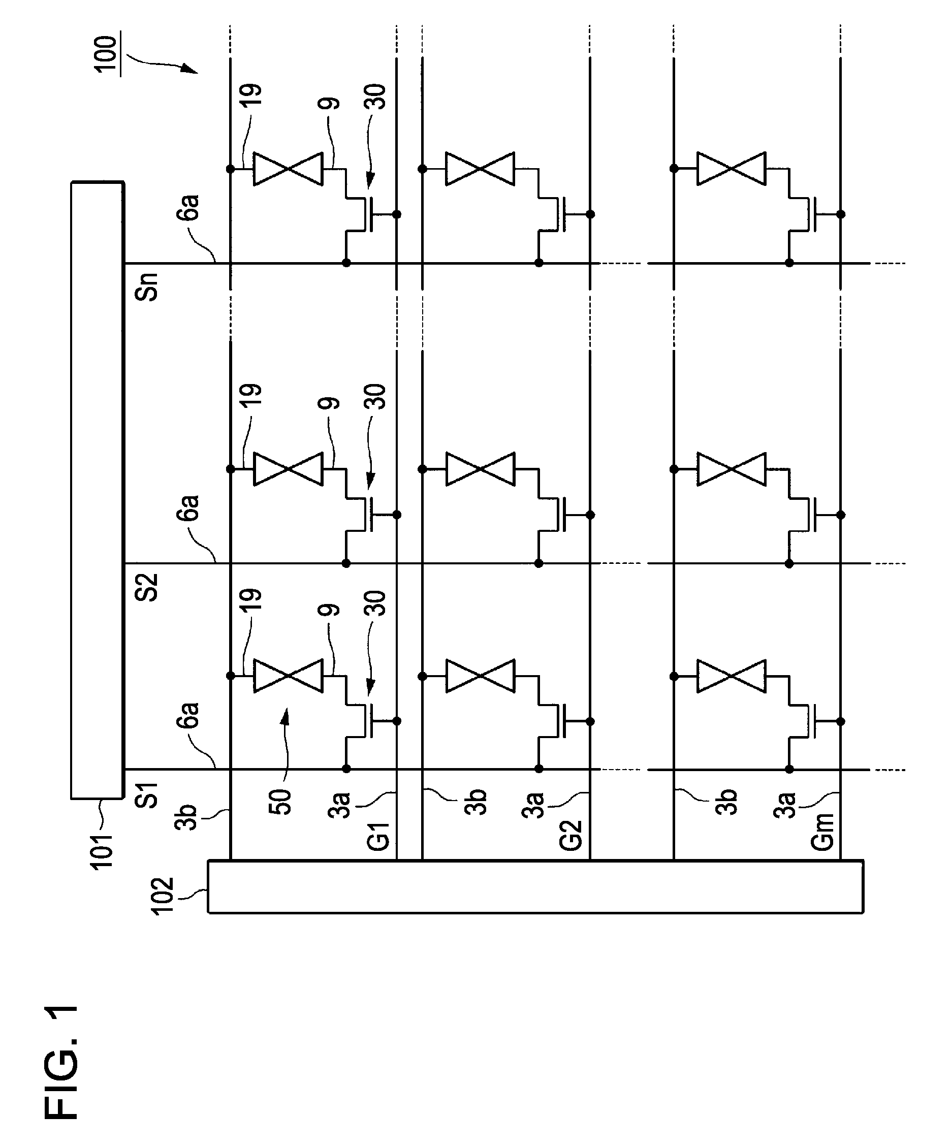
[0033]FIG. 1 is a circuit diagram of a liquid crystal display 100 of this embodiment. In each of a plurality of pixel regions that are arranged in a matrix to form an image display region of the liquid crystal display 100, a pixel electrode 9 and a TFT 30 for switching the pixel electrode 9 are formed. A liquid crystal layer 50 is interposed between the pixel electrode 9 and a common electrode 19. The common electrode 19 is electrically connected to common lines 3b extending from a scanning line driving circuit 102 to hold a plurality of subpixels at a common potential.

[0034]Each of data lines 6a extending from a data line driving circuit 101 is electrically connected to a source of the corresponding TFT 30. The data li...

second embodiment

[0091]FIG. 6 is an explanatory view of a liquid crystal display according to a second embodiment of the invention. A liquid crystal display 200 of this embodiment is partially in common with the liquid crystal display of the first embodiment. A difference is that the phase layer (resin layer) 27 includes an isotropic layer (first resin layer) 27t, which is formed in an isotropic phase state having no optically active direction. Therefore, in this embodiment, the same constituent elements as those in the first embodiment are represented by the same reference numerals, and descriptions thereof will be omitted.

[0092]The isotropic layer 27t is formed in an isotropic phase state. For this reason, light incident on the transmissive display region T is not optically influenced when it transmits the isotropic layer 27t. Therefore, if the alignment direction of the liquid crystal molecules of the liquid crystal layer 50 is set in the same direction as one of the transmission axes of the pola...


PUM


Abstract

A liquid crystal display includes a first substrate and a second substrate opposite to each other with a liquid crystal layer interposed therebetween, first and second electrodes provided on a side of the first substrate facing the liquid crystal layer to drive the liquid crystal layer, and a reflecting layer provided on a part of the side of the first substrate facing the liquid crystal layer. Each pixel region includes a reflective display region where light incoming from the second substrate is reflected by the reflecting layer toward the second substrate to perform display and a transmissive display region where light incoming from the first substrate is transmitted toward the second substrate to perform display. The liquid crystal layer has horizontal alignment in an initial alignment state. A first polarizing plate is provided on a side of the first substrate opposite the liquid crystal layer, the first polarizing plate having a transmission axis parallel or perpendicular to an alignment direction of the liquid crystal layer in the initial alignment state. A second polarizing plate is provided on a side of the second substrate opposite the liquid crystal layer, the second polarizing plate having a transmission axis perpendicular to the transmission axis of the first polarizing plate. A resin layer is provided on a side of the second substrate facing the liquid crystal layer, the resin layer having a first resin layer provided in the transmissive display region and a second resin layer provided in the reflective display region. The first resin layer is a λ/2 phase layer giving a phase difference of approximately ½ wavelength (wavelength: λ) with respect to visible light, and a slow axis of the first resin layer and the transmission axis of the first polarizing plate are disposed so as to be parallel or perpendicular to each other. The second resin layer is a λ/2 phase layer giving a phase difference of approximately ½ wavelength with respect to visible light, and a slow axis of the second resin layer is set in a direction intersecting the alignment direction of the liquid crystal layer. A step portion is provided between the first substrate and the resin layer in order to make the thickness of the liquid crystal layer in the reflective display region smaller than the thickness of the liquid crystal layer in the transmissive display region. A slope portion having a continuously changing thickness is provided in an end portion of the step portion. The slope portion is disposed in the transmissive display region.

Description

BACKGROUND[0001]1. Technical Field[0002]The present invention relates to a liquid crystal display and an electronic apparatus.[0003]2. Related Art[0004]As a light modulation device of various electro-optical devices, a liquid crystal display is used, and in recent years, it is widely used for various purposes. Such a liquid crystal display includes a transflective liquid crystal display which includes a reflective display mode using external light and a transmissive display mode using an internal light source, such as a backlight, as a display mode. The transflective liquid crystal display selectively uses one display mode of a reflective mode and a transmissive mode in accordance with ambient brightness. In this case, power consumption can be reduced, and clear display can be performed even in the dark.[0005]In the transflective liquid crystal display, a phase difference is likely to be produced between a region for reflective display (reflective display region) and a region for tr...

Claims


Application Information

Patent Timeline
IPC IPC(8): G02F1/1335
CPCG02F1/133371G02F1/133555G02F1/134363G02F2413/09G02F2413/01G02F2413/08G02F2001/133638G02F1/133631G02F1/133638
Inventor TSUCHIYA, HITOSHI
Owner JAPAN DISPLAY WEST
Why Eureka
Try Eureka