Heat treatment apparatus and method for heating substrate by light irradiation

Active Publication Date: 2009-10-22
DAINIPPON SCREEN MTG CO LTD
View PDF9 Cites 24 Cited by
  • Summary
  • Abstract
  • Description
  • Claims
  • Application Information

AI Technical Summary

Benefits of technology

[0019]Since the surface temperature of the substrate will never considerably exceed its temperature initially raised, possible damage to the substrate can be prevented with reli

Problems solved by technology

The occurrence of such a phenomenon gives rise to apprehension that the junction may become deeper than the desired level, hindering good device formation.
Now, as a result of the high-energy ion implantation prior to the flash heating, a number of defects are introduced into a silicon crystal of a semiconductor wafer.
However, there ar

Method used


Image

  • Heat treatment apparatus and method for heating substrate by light irradiation
  • Heat treatment apparatus and method for heating substrate by light irradiation
  • Heat treatment apparatus and method for heating substrate by light irradiation

Examples


Embodiment Construction

[0032]A preferred embodiment of the invention is now described in detail with reference to the drawings.

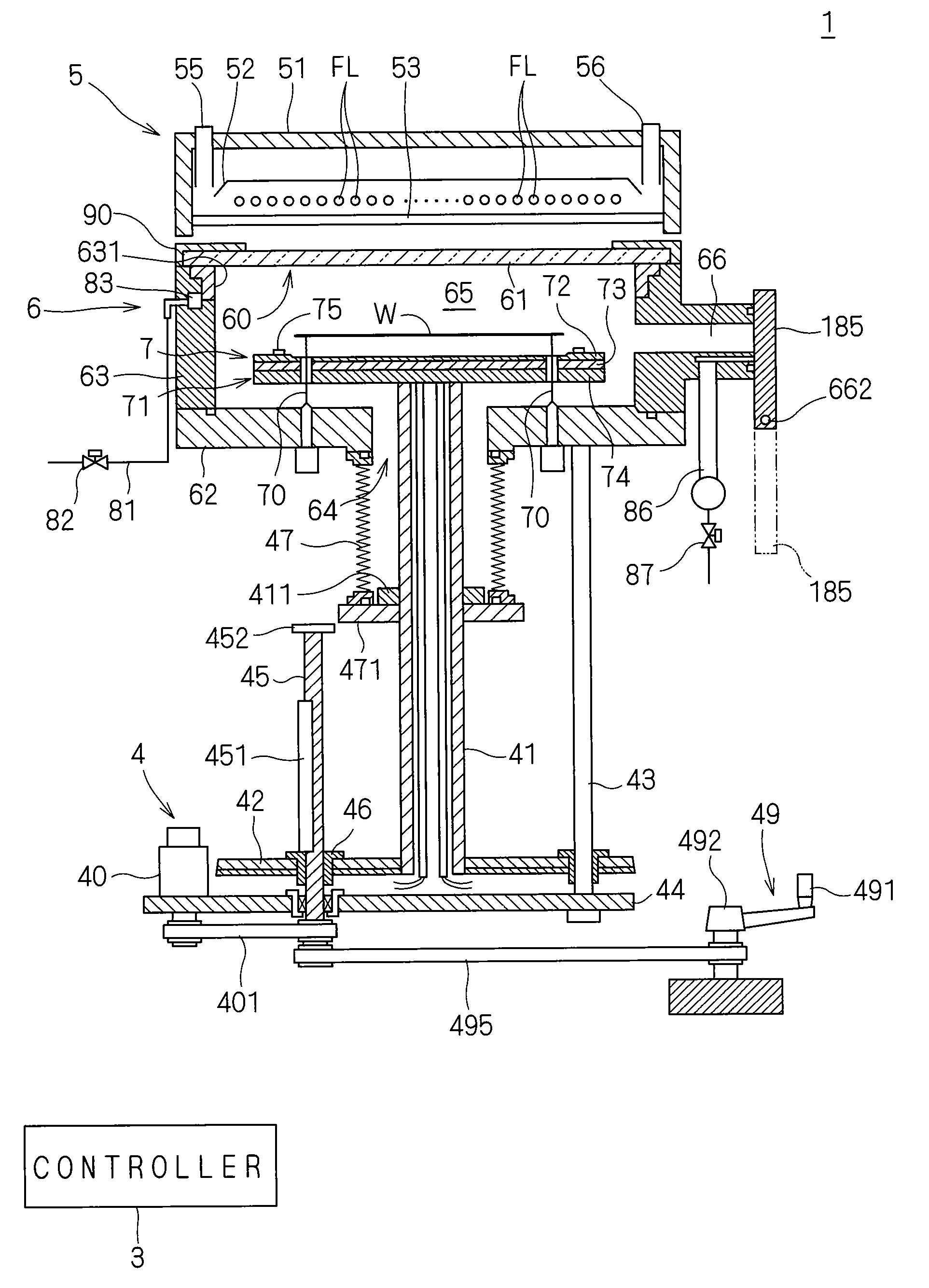
[0033]First, a general configuration of a heat treatment apparatus according to the invention is outlined. FIG. 1 is a side sectional view of a configuration of a heat treatment apparatus 1 according to the invention. The heat treatment apparatus 1 shall be a lamp annealer for applying light to a generally disc-shaped semiconductor wafer W serving as a substrate to thereby heat the semiconductor wafer W.

[0034]The heat treatment apparatus 1 includes a generally-cylindrical chamber 6 for receiving a semiconductor wafer W therein; and a lamp house 5 including a plurality of built-in flash lamps FL. The heat treatment apparatus 1 further includes a controller 3 for controlling each operating mechanism provided in the chamber 6 and in the lamp house 5 for the implementation of the heat treatment of a semiconductor wafer W.

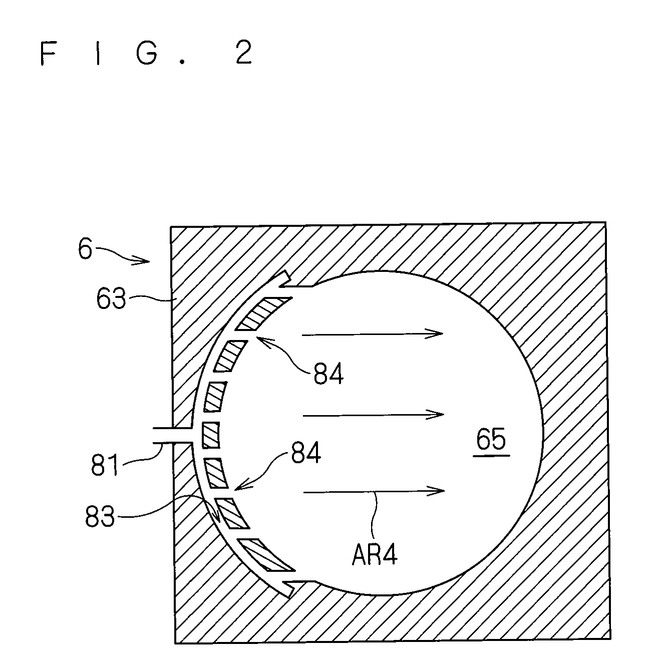
[0035]The chamber 6 is located below the lamp house 5 and includ...


PUM

PropertyMeasurementUnit
Timeaaaaaaaaaa
Timeaaaaaaaaaa
Timeaaaaaaaaaa

Abstract

In light-irradiation heating with a total irradiation time of one second or less, two-stage irradiation is performed, including a first stage of light irradiation of a semiconductor wafer, which irradiation produces an output waveform that reaches a peak at a given emission output; and a second stage of supplemental light irradiation of the semiconductor wafer, which irradiation is started after the peak, producing an emission output smaller than the above given emission output. The emission output in the second stage is two thirds or less than the above given emission output at the peak. The first-stage light-irradiation time is between 0.1 and 10 milliseconds, and the second-stage light-irradiation time is 5 milliseconds or more. This allows the temperature of the semiconductor wafer even at a somewhat greater depth below the surface to be raised to some extent while allowing the surface temperature to be maintained at a generally constant processing temperature.

Description

BACKGROUND OF THE INVENTION[0001]1. Field of the Invention[0002]The present invention relates to a heat treatment apparatus and method for heating a semiconductor wafer, a glass substrate for liquid crystal display, and the like (hereinafter referred to simply as a “substrate”) by light irradiation of the substrate.[0003]2. Description of the Background Art[0004]Conventionally, a lamp annealer employing halogen lamps has been commonly used in the step of activating ions in a semiconductor wafer after ion implantation. Such a lamp annealer carries out the activation of ions in a semiconductor wafer by heating (or annealing) the semiconductor wafer to a temperature of the order of, for example, 1000 to 1100° C. In such a heat treatment apparatus, the energy of light emitted from halogen lamps is used to raise the substrate temperature at a rate of about several hundred degrees per second.[0005]In recent years, with increasing degree of integration of semiconductor devices, it has been...

Claims


Application Information

Patent Timeline
IPC IPC(8): F26B3/30
CPCH01L21/67115
Inventor KIYAMA, HIROKIYOKOUCHI, KENICHI
Owner DAINIPPON SCREEN MTG CO LTD
Why Eureka
Try Eureka