

Intersect area based ground rule for semiconductor design
a technology of inter-area area and ground rule, applied in the field of inter-area based ground rule for semiconductor design, can solve the problems of time-consuming and/or difficult understanding of ground rule, limitations between the various elements of design data, and limitations on the shape in a design level, so as to achieve the effect of optimizing the design data
- Summary
- Abstract
- Description
- Claims
- Application Information
AI Technical Summary
Benefits of technology
Problems solved by technology
Method used
Image

Examples
Embodiment Construction
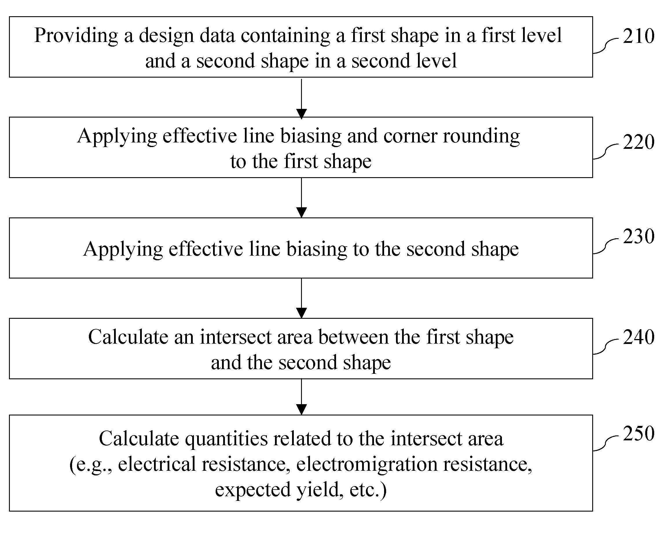
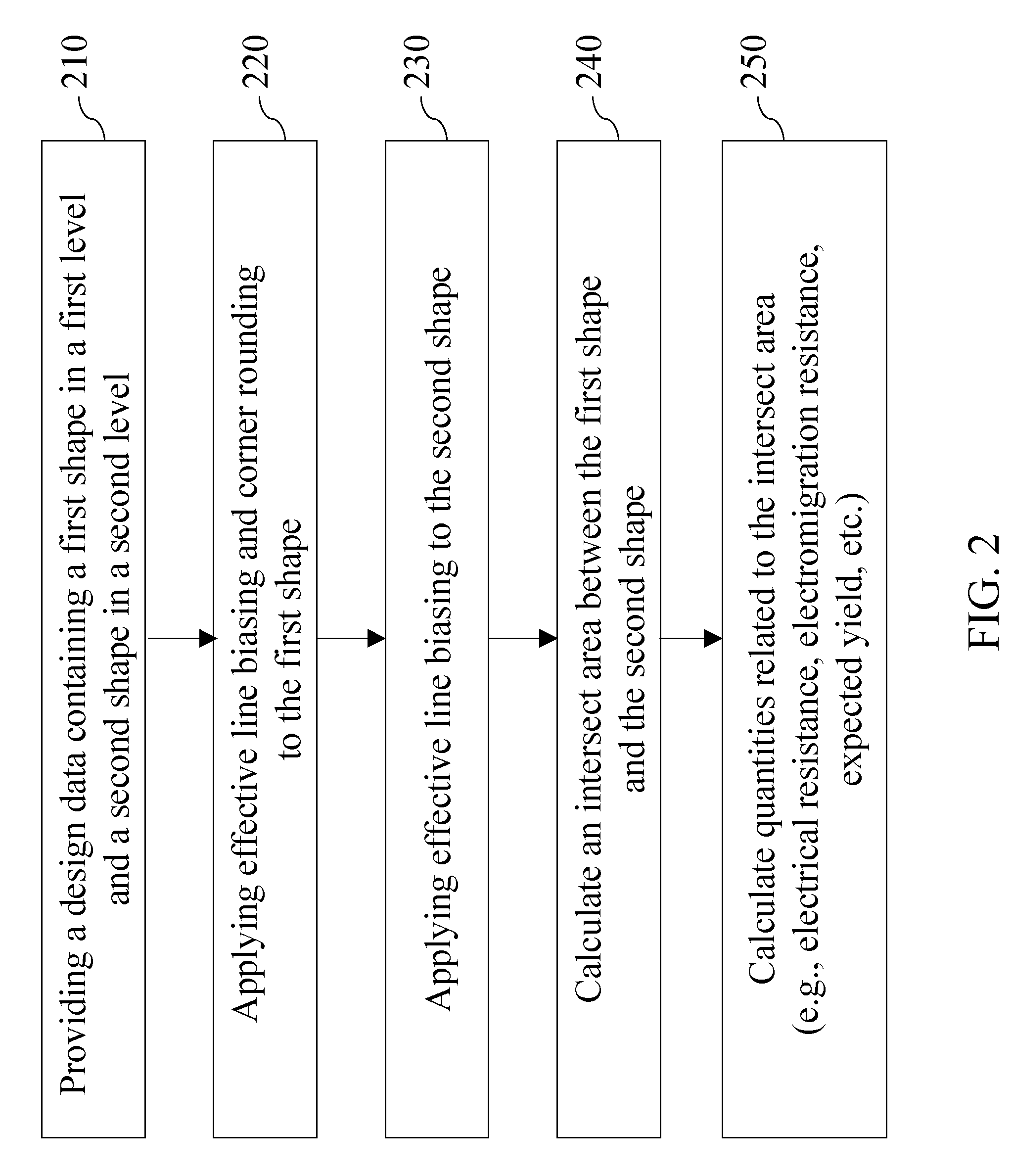
[0032]As stated above, the present invention relates to a method of providing a model calculation for a semiconductor design employing a ground rule based on an intersect area calculation between vertically adjoining levels, and to a semiconductor design methodology, and particularly, to a semiconductor design methodology employing a ground rule based on such an intersect area calculation for checking and / or improving a semiconductor device design, which are now described in detail with accompanying figures. It is noted that like reference numerals refer to like elements or like steps.
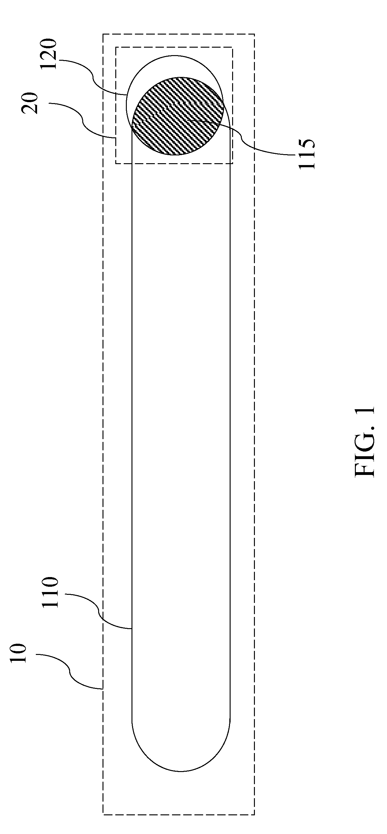
[0033]Referring to FIG. 1, a first design shape 10 and a second design shape 20 in a design dataset is shown. The first design shape 10 resides, that is, is present within a class of design shapes belonging to, a first design level and the second design shape 20 resides in a second design level. The first design level and the second design level are different. The first design level and the second desi...
PUM
 Abstract
Description
Claims
Application Information