Semiconductor chip having TSV (through silicon via) and stacked assembly including the chips

a technology of semiconductor chips and stacked assemblies, which is applied in the direction of semiconductor devices, semiconductor/solid-state device details, electrical apparatus, etc., can solve the problems of chip deformation or warpage, easy breakage of electrical connections formed by stud bumps located between the chips, and easy breakage of electrical connections of tsv. to achieve the effect of accurate alignment of semiconductor chips 300

Inactive Publication Date: 2009-10-29
POWERTECH TECHNOLOGY
View PDF8 Cites 97 Cited by
  • Summary
  • Abstract
  • Description
  • Claims
  • Application Information

AI Technical Summary

Benefits of technology

[0036]As shown in FIG. 10, when vertically stacking a plurality of semiconductor chips 300 with different dimensions, the second surfaces 312 face to the same direction when vertically stacking chips such as facing toward the carrier 30 where the second extruded rings 350 on the second surface 312 of the semiconductor substrate 310 stacked on top are aligned and inserted into the first extruded rings 340 on the first surface 311 of another semiconductor subst...

Problems solved by technology

However, each chip will generate heat during operation, therefore, the induced thermal stresses will cause the chip to deform or to warpage and even to break the electrical connections of TSV where stresses are concentrated.
However, when the chip experiences thermal stresses causing deformation or warpage, the electrical connections formed by the stud bumps located between ...

Method used


Image

  • Semiconductor chip having TSV (through silicon via) and stacked assembly including the chips
  • Semiconductor chip having TSV (through silicon via) and stacked assembly including the chips
  • Semiconductor chip having TSV (through silicon via) and stacked assembly including the chips

Examples


first embodiment

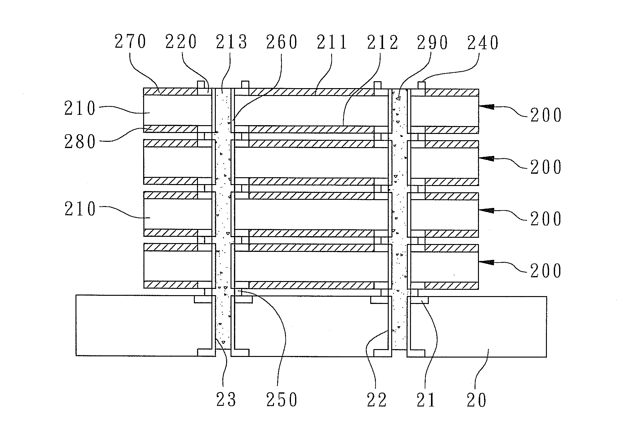
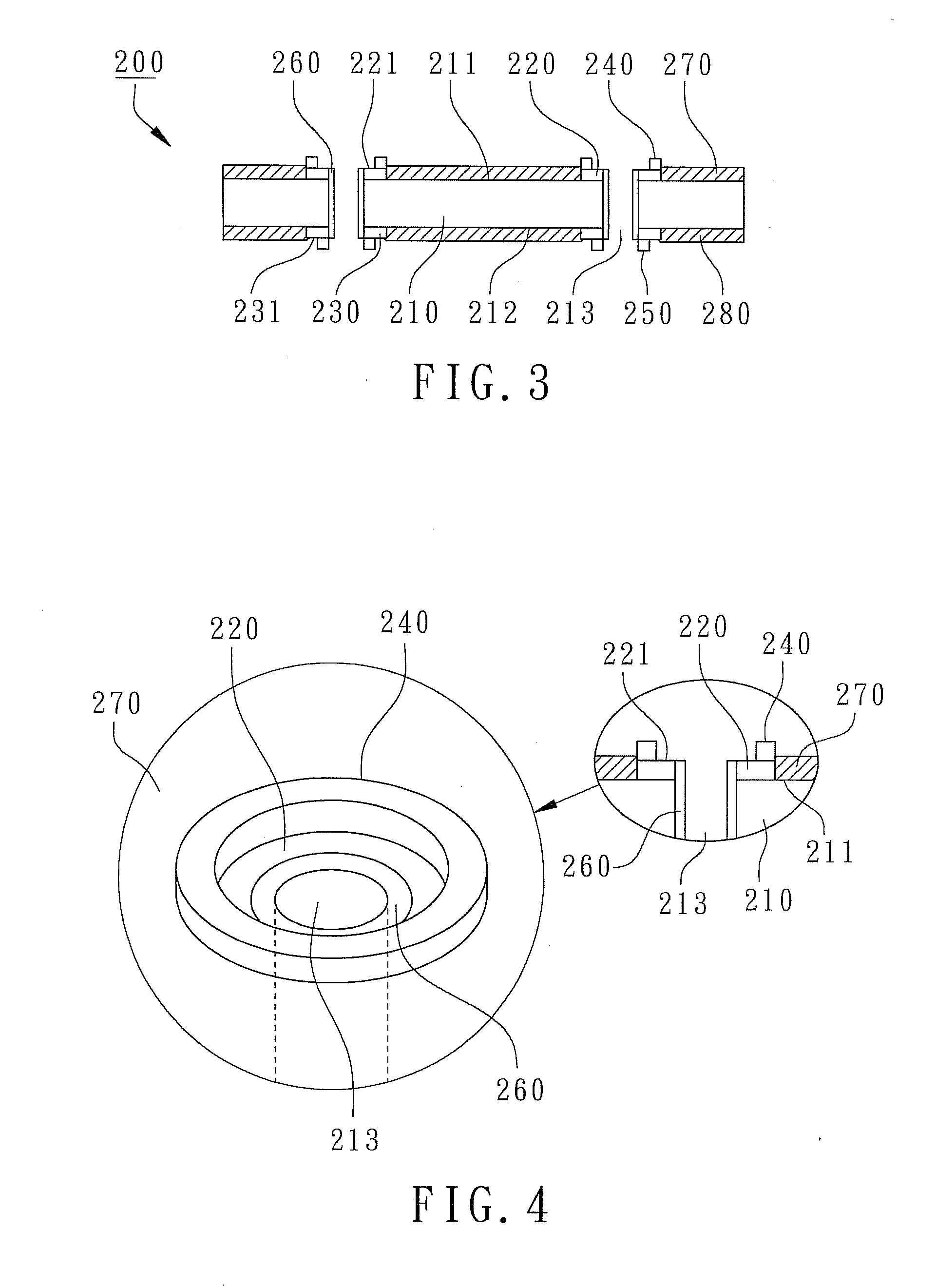
[0021]the semiconductor chip having TSV of the present invention is illustrated in the cross-sectional view of FIG. 3. The semiconductor chip 200 with TSV configuration primarily comprises a semiconductor substrate 210, a plurality of first bonding pads 220, a plurality of second bonding pads 230, a plurality of first extruded rings 240, and a plurality of second extruded rings 250. The semiconductor substrate 210 has a first surface 211, a corresponding second surface 212, and a plurality of through holes 213 penetrating from the first surface 211 to the second surface 212. The semiconductor substrate 210 is made of semiconductor materials such as Si, GaAs, etc. Various ICs are formed on one surface of the semiconductor substrate 210 and electrically connected to a plurality of first bonding pads 220 and to a plurality of second bonding pads 230. Therein, the surface on which ICs are formed is an active surface. Preferably, the ICs are formed on the second surface 212 of the semico...

second embodiment

[0030]the semiconductor chip having TSV of the present invention is illustrated in the cross-sectional view of FIG. 8. A stacked assembly including the chips is illustrated in the cross-sectional view of FIG. 9 and FIG. 10. The semiconductor chip 300 primarily comprises a semiconductor substrate 310, at least a first bonding pad 320, at least a second bonding pad 330, at least a first extruded ring 340, and at least a second extruded ring 350. The semiconductor substrate 310 has a first surface 311, a corresponding second surface 312, a first blind hole 313 in the first surface 211, and a second blind hole 314 in the second surface 212. To be more specific, the first blind hole 313 and the second blind hole 314 are blind vias formed by half-etching and plating, not penetrating through the semiconductor substrate 310. The first bonding pad 320 is disposed on the first surface 311 of the semiconductor substrate 310 with the first blind hole 313 penetrating through the first bonding pa...


PUM


Abstract

A semiconductor chip having through silicon vias (TSV) and a stacked assembly including the chip are revealed. The chip has a plurality of first and second bonding pads disposed on two opposing surfaces of a semiconductor substrate respectively. Through hole vertically penetrate through the semiconductor substrate and the first and second bonding pads. By forming first extruded ring, the first bonding pad has a first contact surface located between the first extruded ring and the through hole. By forming second extruded ring, the second bonding pad has a second contact surface located outside and adjacent to the second extruded rings to encircle the second extruded ring. The second extruded ring has a proper dimension to fit in the first extruded ring. Accordingly, a plurality of semiconductor chip can be stacked each other with accurate alignment without shifting to effectively reduce the stacked assembly height, moreover, chip stacking processes are accomplished by vertically stacking a plurality of chips first then filling conductive material into the through holes without electrical short between the adjacent bonding pads due to overflow of conductive material to meet the fine-pitch requirements of TSV. The process flow for the stacked assembly is simplified with higher production yields.

Description

FIELD OF THE INVENTION[0001]The present invention relates to semiconductor devices, especially to a semiconductor chip having TSV (Through Silicon Via) and a stacked assembly including the chips.BACKGROUND OF THE INVENTION[0002]In conventional semiconductor chips, ICs are formed on the active surfaces of the semiconductor chips with conventional electrical terminals such as bonding pads formed on the active surface. In high-density electrical interconnections, 3D chip stacking was developed with electrical terminals not only disposed on the active surfaces but also on the corresponding back surfaces of the semiconductor chips. Through Silicon Via (TSV) is the enabled technology to vertically stack several chips to assemble 3D chip stacking packages or modules with high powers, high densities, and smaller dimensions. TSV's are electrically-conductive through holes inside a chip penetrating through the top surface and the bottom surface of a chip to create vertical electrical connecti...

Claims


Application Information

Patent Timeline
IPC IPC(8): H01L23/488
CPCH01L21/76898H01L2924/01029H01L25/0657H01L2225/06513H01L2225/06517H01L2225/06527H01L2224/08235H01L2224/80141H01L24/05H01L24/80H01L24/92H01L2224/06181H01L2224/08146H01L2224/9202H01L2225/06565H01L2225/06562H01L2224/08245H01L2924/00013H01L23/481H01L2224/13099H01L2224/13599H01L2224/05599H01L2224/05099H01L2224/29099H01L2224/29599H01L2924/351H01L2924/15787H01L2924/00
Inventor CHEN, MING-YAO
Owner POWERTECH TECHNOLOGY
Why Eureka
Try Eureka