Driving method for solid-state imaging device and solid-state imaging device

a solid-state imaging and driving method technology, applied in the direction of instruments, television systems, color signal processing circuits, etc., can solve the problems of not providing the technical features of substantial image quality improvement such as a dynamic range, and the dynamic range of the image obtained by subtracting the dark signals with respect, so as to improve imaging fidelity and signal processing time, reduce noise, and improve image quality

Active Publication Date: 2009-10-29
PANASONIC SEMICON SOLUTIONS CO LTD
View PDF8 Cites 7 Cited by
  • Summary
  • Abstract
  • Description
  • Claims
  • Application Information

AI Technical Summary

Benefits of technology

[0022]In view of the above problems, the present invention provides a driving method for solid-state imaging device and a solid-state imaging device that are used for improving imaging fidelity and a signal processing time by reducing noise due to dark signals generated in the peripheral circuitry.
[0023]In order to solve the above problems, a driving method for use in a solid-state imaging device according to the present inventions is a driving method for use in a solid-state imaging device which includes a solid-state image sensor including an imaging region and a peripheral circuitry arranged around the imaging region, and which includes: imaging an object for a first storage time in a period when a shutter is open, in a first state that is a state where either at least a part of the peripheral circuitry is suspended or a consumption current of the peripheral circuitry is limited; reading a signal image of the imaged object in a second state that is a state where the peripheral circuitry is not suspended and the consumption current is not limited; imaging, in the first state, a dark output signal image including only a dark output for a second storage time in a period when the shutter is closed; reading the imaged dark output signal image in the second state; and converting the dark output signal image to correspond to the image obtained for the first storage time and subtracting, from the signal image of the object, the converted dark output signal image or converting the dark output signal image to correspond to the image obtained for the second storage time and subtracting, from the signal image of the object, the converted dark output signal image. As this configuration suppresses dark outputs generated in the peripheral circuitry at the time of imaging the object and dark outputs due to emission of light by especially DAHCs, an amount of compensation of the dark outputs is less than before. Thus, it is possible to reduce deterioration in image quality caused by the compensation of the dark outputs due to the peripheral circuitry.
[0024]Furthermore, the driving method for use in the solid-state imaging device is a driving method for use in a solid-state imaging device which includes a solid-state image sensor including an imaging region and a peripheral circuitry arranged around the imaging region, and which may include: imaging a first dark output signal image including only a dark output for a first storage time in a period when a shutter is closed, in a first state that is a state where either at least a part of the peripheral circuitry is suspended or a consumption current of the peripheral circuitry is limited; reading the imaged first dark output signal image in a second state that is a state where the peripheral circuitry is not suspended and the consumption current is not limited; reading, in the second state, a second dark output signal image that includes only a dark output and is imaged for a second storage time in a period when the shutter is closed; generating a third dark output signal image by converting the first dark output signal image to correspond to the second dark output signal image obtained for the second storage time and by subtracting, from the second dark output signal image, the converted the first dark output signal image; imaging, in the second state, an object for a third storage time in a period when the shutter is open, and reading a signal image of the object; and converting the third dark output signal image to correspond to the signal image obtained for the third storage time, and subtracting, from the signal image of the object, the converted third dark output signal image. With this configuration, since only the dark outputs due to the DAHCs of the peripheral circuitry and having small temperature dependence can be compensated, it is possible to attempt shortening an effective imaging time (that is, elimination of an imaging-restricted period) while maintaining the certain effect of the compensation. This is because, as the third dark output signal image is an image indicating only the dark output components due to the DAHCs, the third dark output signal image can be prepared in advance before the imaging time of the object.
[0025]Here, a substrate of the solid-state image sensor may have a thickness of no more than 500 μm. With this configuration, in the case where the thickness of the substrate is no more than 500 μm at which the dark outputs due to the DAHCs increase, a compensation effect for the dark outputs due to the DAHCs can be greatly produced.
[0026]Here, the solid-state imaging device may include a temperature sensor that detects a temperature of either the solid-state image sensor or a periphery of the solid-state image sensor, and the driving method may further include determining an imaging mode for imaging the object based on the temperature detected by the temperature sensor. With this configuration, as the temperature sensor detects a temperature of the solid-state image sensor or a vicinity of the solid-state image sensor and an imaging mode suitable to the detected temperature is determined, a dynamic range can be improved through suppression of the dark outputs generated at the time of imaging.

Problems solved by technology

Even this method does not differ from the conventional methods in that the compensation is performed by subtracting, from an imaged image, dark signals predicted to be generated in an approximate imaging exposure time, and there is a problem that a dynamic range of the image obtained by subtracting the dark signals deteriorates with respect to an original dynamic range of a solid-state image sensor since the dark outputs increase in direct proportion to the exposure time.
Although the conventional technique disclosed in Patent Reference 2 produces an advantageous effect that a person imaging recognizes deterioration in image quality in advance, the conventional technique has a problem that technical features for substantial image quality improvement such as a dynamic range are not provided.

Method used


Image

  • Driving method for solid-state imaging device and solid-state imaging device
  • Driving method for solid-state imaging device and solid-state imaging device
  • Driving method for solid-state imaging device and solid-state imaging device

Examples


embodiment 1

[0061]The following will describe a driving method for solid-state imaging device and a solid-state imaging device according to Embodiment 1 of the present invention.

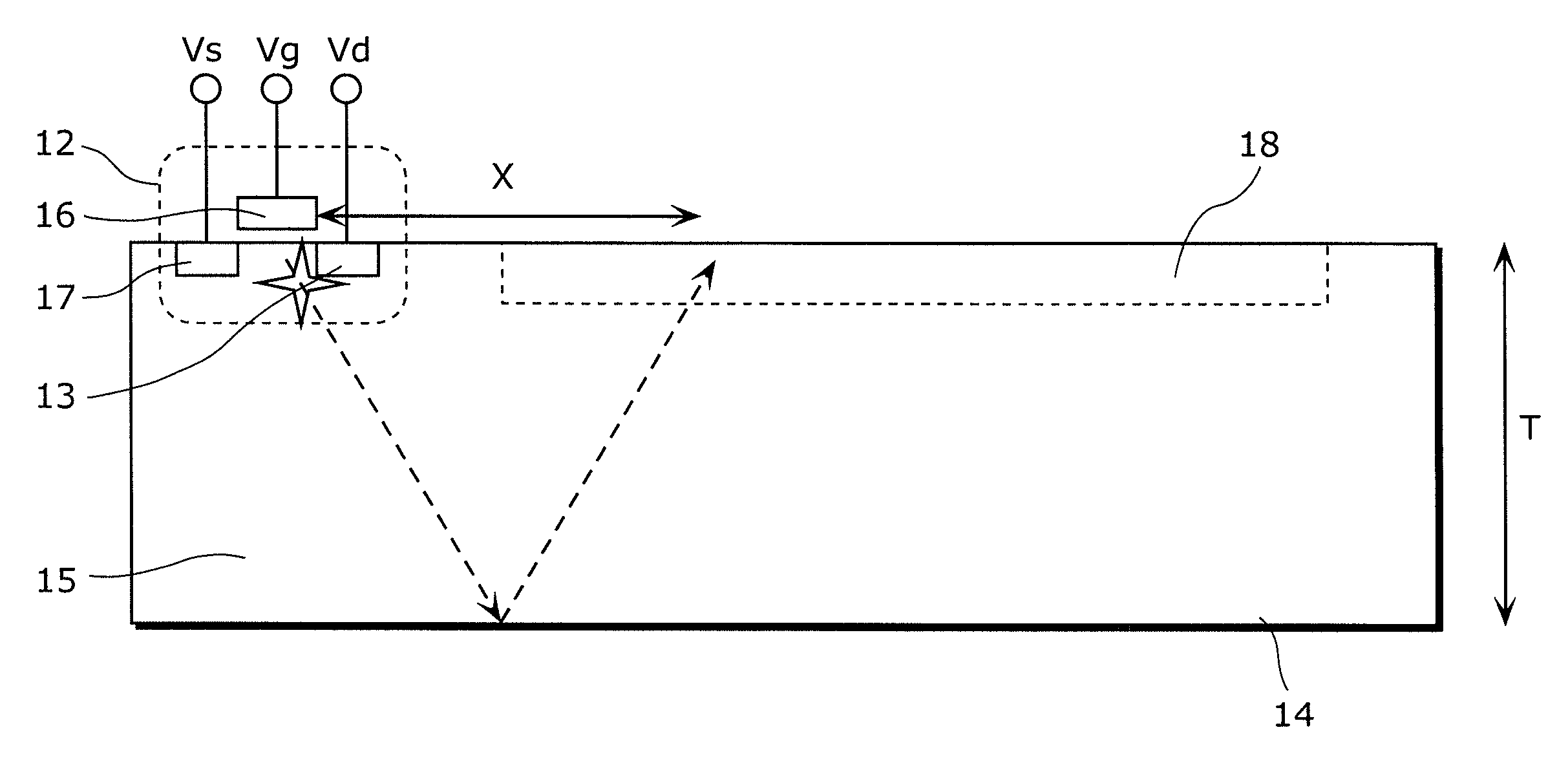
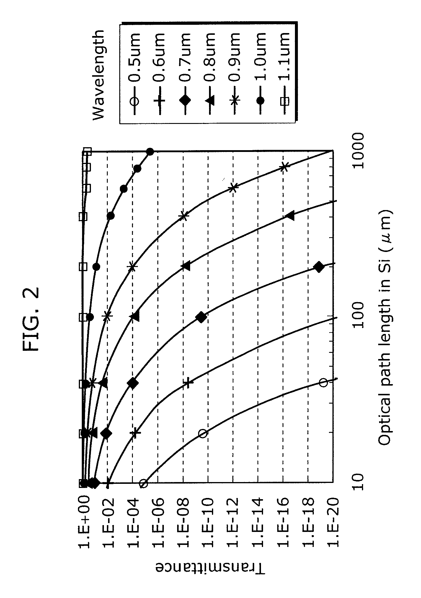
[0062]FIG. 1 is a schematic sectional diagram of a solid-state image sensor included in a solid-state imaging device. It is to be noted that in order to facilitate understanding of the present invention with FIG. 1, a peripheral circuitry (including one or more peripheral circuits) of the solid-state image sensor is represented by a single MOS transistor. In FIG. 1, a solid-state image sensor 14 includes a semiconductor substrate 15, and a peripheral circuitry 12 and an imaging region 18 that are formed on the semiconductor substrate 15; and the peripheral circuitry 12 includes a drain 13, a gate 16, and a source 17. The semiconductor substrate 15 is usually made of Si single crystal. Furthermore, T represents a thickness of the semiconductor substrate 15, and x represents a distance from the drain 13 to photodiodes. A ...

embodiment 2

[0091]The following will describe a driving method for solid-state imaging device according to Embodiment 2 of the present invention with reference to the drawings.

[0092]FIG. 10 is a diagram showing the driving method for solid-state imaging device according to the present invention.

[0093]The present embodiment provides a different driving method for use in the solid-state imaging device shown in FIG. 6 in Embodiment 1.

[0094]In the driving method for solid-state imaging device according to the present embodiment, a dark output image due to an operation of a peripheral circuitry is extracted and stored in a solid-state imaging device in advance according to the following procedure. In other words, the procedure is performed as follows. The peripheral circuitry is first activated as usual. Next, a shutter is closed (S101), and a first dark output image is obtained through signal accumulation for a certain period in a light-shielded state (S102). The peripheral circuitry is subsequentl...

embodiment 3

[0103]The following will describe a driving method for solid-state imaging device and a solid-state imaging device according to Embodiment 3 of the present invention with reference to the drawings.

[0104]FIG. 13 is a diagram showing the solid-state imaging device according to the present embodiment. The solid-state imaging device according to the present embodiment differs from the solid-state imaging device according to Embodiment 1 shown in FIG. 6 in including a temperature sensor 70 and an imaging mode control device 71.

[0105]FIG. 14 is a diagram showing a conventional driving method for solid-state imaging device. This conventional method (S141 to S146) in which a peripheral circuitry is not suspended and dark outputs are not compensated is called an imaging mode 4. Since the peripheral circuitry is not switched on and off in this mode, the mode is suitable for continuous imaging or a condition where the dark outputs are not high.

[0106]FIG. 15 is a diagram showing the driving met...


PUM


Abstract

A driving method used for a solid-state imaging device according to the present invention includes: imaging an object for a first storage time when a shutter is open, in a first state that is a state where either at least a part of the peripheral circuitry is suspended or a consumption current of the peripheral circuitry is limited; imaging, in the first state, a dark output signal image including only a dark output for a second storage time when the shutter is closed; converting the dark output signal image to correspond to the image obtained for the first storage time and subtracting, from the signal image of the object, the converted dark output signal image or converting the dark output signal image to correspond to the image obtained for the second storage time and subtracting, from the signal image of the object, the converted dark output signal image.

Description

BACKGROUND OF THE INVENTION[0001](1) Field of the Invention[0002]The present invention relates to a driving method for solid-state imaging device and a solid-state imaging device that improve fidelity of imaging and a signal processing time through noise reduction caused by a dark signal generated in a peripheral circuitry.[0003](2) Description of the Related Art[0004]CCDs and MOS image sensors are generally used as solid-state image sensors in digital cameras, video cameras, and the like. The solid-state image sensors have been improved in recent years, and high-resolution solid-state image sensors have come to allow high-definition images to be imaged.[0005]That dark currents caused by crystal defects in pixels are a factor for reducing the quality of the imaged images is known as the characteristics of the aforementioned solid-state image sensors.[0006]Although dark outputs of the solid-state image sensors have been reduced, when imaging through long exposure exceeding several se...

Claims


Application Information

Patent Timeline
Patent Type & Authority Applications(United States)
IPC IPC(8): H04N5/335H04N5/353H04N5/355H04N5/357H04N5/372H04N5/374H04N5/378
CPCH04N5/361H04N5/335H04N25/00H04N25/63
Inventor TSUKAMOTO, AKIRAKOHNO, AKIYOSHI
Owner PANASONIC SEMICON SOLUTIONS CO LTD
Why Eureka
Try Eureka