MEMS galvanometer laser micro-display

A microdisplay and laser technology, applied in optics, instruments, optical components, etc., can solve problems such as image pincushion distortion, and achieve the effects of low cost, good safety performance, and low energy consumption

Active Publication Date: 2018-09-25
SUZHOU INST OF NANO TECH & NANO BIONICS CHINESE ACEDEMY OF SCI
View PDF6 Cites 3 Cited by
  • Summary
  • Abstract
  • Description
  • Claims
  • Application Information

AI Technical Summary

Problems solved by technology

In an existing MEMS galvanometer micro-projection system, red light (red) and blue light (blue) use semiconductor lasers, and green light (green) uses frequency-doubled solid-state lasers. Its working principle is to output three-color lasers The light spot is first collimated (or converged) and then beam-combined before being incident on the MEMS mirror, reflected by the MEMS galvanometer and directly projected onto the display screen, but since the usual display screen is flat, the MEMS galvanometer scans a curved surface , leading to severe pincushion distortion in the image

Method used


Image

  • MEMS galvanometer laser micro-display
  • MEMS galvanometer laser micro-display
  • MEMS galvanometer laser micro-display

Examples


Embodiment 1

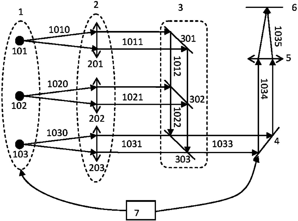
[0130] Example 1: See figure 2 It is a structural schematic diagram of a MEMS galvanometer laser microdisplay in the first embodiment of the present invention. The structure and the structure of the MEMS galvanometer laser microdisplay in this embodiment figure 1 The structures shown are essentially the same. Since the divergence angles of semiconductor lasers in the fast axis and slow axis directions are different, in order to obtain a circular spot with good collimation effect, it is necessary to collimate the light beams in the fast axis and slow axis directions respectively. In this embodiment 1, the collimating and shaping optical system 2 (that is, the laser collimating and shaping optical path) is completed by a single irregular lens, and the single irregular lens is a cylindrical surface whose two front and rear faces are orthogonal, and the curvature is aspherical. The first surface 11 of the single irregular lens adopts a convex structure. In the direction of th...

Embodiment 2

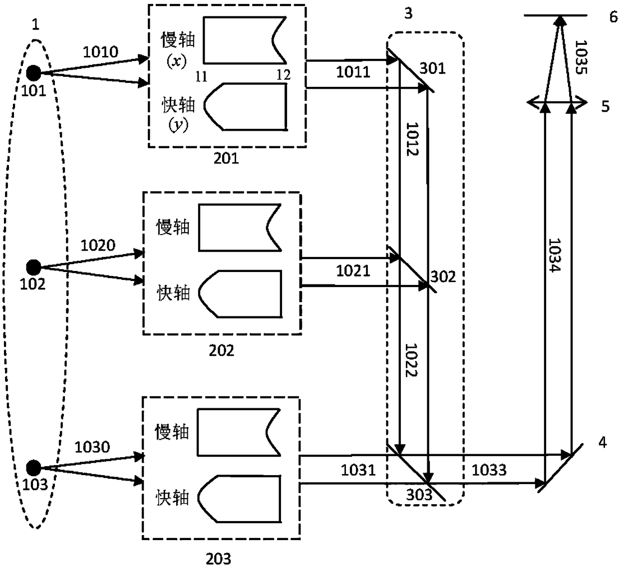
[0131] Example 2: image 3 It is a structural schematic diagram of a MEMS galvanometer laser microdisplay in the second embodiment of the present invention. The structure of the MEMS galvanometer laser microdisplay in this embodiment is basically the same as that of Embodiment 1, the only difference is that the collimation and shaping optical system uses two lenses to realize the collimation and shaping of the laser beam, wherein the first lens is not Regular structure, the second lens is plano-convex structure. In Embodiment 2, the first surface 21 of the first lens adopts a rotating aspheric surface, and the surface 21 realizes the collimation of the fast-axis and slow-axis beams at the same time, so the shape of the beam emitted from the surface 21 is a collimated and parallel elliptical spot . The second surface 22 of the first lens and the first surface 23 of the second lens are all aspheric surfaces in the slow axis direction, and both (face 22 and surface 23) form a G...

Embodiment 3

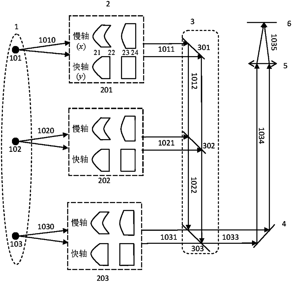
[0132] Example 3: Figure 4 It is a structural schematic diagram of a MEMS galvanometer laser microdisplay in the third embodiment of the present invention. The structure of the MEMS galvanometer laser microdisplay in this embodiment is basically the same as in Embodiment 2, the only difference is that the collimation and shaping optical system uses three lenses to realize the collimation and shaping of the laser beam, and the three lenses all adopt a plano-convex structure. In Embodiment 3, the first surface 31 of the first lens is the same as the first surface 21 of the first lens in Embodiment 2, that is, the surface 31 can also realize the collimation of the fast-axis and slow-axis light beams at the same time . Both the second surface 34 of the second lens and the first surface 35 of the third lens are aspherical in the direction of the slow axis, and they form a Kepler telescope structure to realize beam expansion in the direction of the slow axis. The remaining faces ...


PUM


Abstract

The invention discloses an MEMS galvanometer laser micro-display, which comprises a laser light source and a beam combining system, wherein the laser light source a green-light semiconductor laser light source, a blue-light semiconductor laser light source and a red-light semiconductor laser light source which are respectively used for emitting a green light beam, a blue light beam and a red lightbeam; and the beam combining system comprises a shaping lens group, a beam combining mechanism, an MEMS galvanometer and a control unit, the shaping lens group is at least used for shaping the greenlight beam, the blue light beam and the red light beam emitted by the laser light source, the beam combining mechanism is used for combining the shaped green light beam, blue light beam and red lightbeam into one light beam; the MEMS galvanometer is at least used for reflecting the RGB combined light beam outputted by the beam combining system, forming a parallel light beam or a convergent lightbeam and shooting the parallel light beam or convergent light beam into a display unit; and the control unit is at least used for controlling the light intensity change of the laser light source and the operating state of the MEMS galvanometer. Images formed on the MEMS galvanometer laser micro-display are high in authenticity. In addition, the MEMS galvanometer also has the advantages of small size, low energy consumption, low cost, good safety and the like.

Description

technical field [0001] The invention relates to a microdisplay used in a head-mounted display, in particular to a laser microdisplay using a laser light source and a MEMS vibrating mirror. Background technique [0002] A helmet mounted display (HMD) is a miniature device installed on a helmet to generate a visual virtual image for the helmet user. The helmet-mounted display was originally designed to enable the weapon system to quickly lock the target with the pilot's actions in air combat, thereby improving combat efficiency. After several decades of development, the scope of the head-mounted display has expanded from the initial military aspect to daily life (such as mobile phones, vehicle instrumentation displays). [0003] From the perspective of the optical system, the helmet display system is mainly composed of two parts, one is the micro-display system, and the other is the visual optical system. The micro-display system converts the video signal incident from the ou...

Claims


Application Information

Patent Timeline
Patent Type & Authority Applications(China)
IPC IPC(8): G03B21/00G03B21/20G02B27/14G02B27/01
CPCG02B27/0101G02B27/14G03B21/008G03B21/2033G03B21/208
Inventor 李敏吴东岷沈文江
Owner SUZHOU INST OF NANO TECH & NANO BIONICS CHINESE ACEDEMY OF SCI
Why Eureka
Try Eureka