Flexible device, flexible pressure sensor, and fabrication method thereof

a flexible device and sensor technology, applied in the direction of fluid pressure measurement, printed circuit non-printed electric components association, instruments, etc., can solve the problems of not being directly used by users, prone to breakage, and limit in making it small and thin

Active Publication Date: 2009-11-05
SAMSUNG ELECTRONICS CO LTD
View PDF3 Cites 63 Cited by
  • Summary
  • Abstract
  • Description
  • Claims
  • Application Information

AI Technical Summary

Benefits of technology

[0009]It is therefore one object of the present invention to provide a flexible device having a high flexibility, a flexible pressure sensor, and a fabrication method thereof.
[0030]The method may further include depositing another flexible substrate on the coil, the another flexible substrate being formed of a flexible material to have a flexibility and allowing a circular shape to be formed when it is bent.

Problems solved by technology

Semiconductor devices (e.g. chips) fabricated on a wafer are electrical devices, however, they may be not directly used by users and are apt to be broken.
In order to implement a small-sized semiconductor package device, it may be fabricated to be small and thin, however, which causes it to be readily broken, so that there exists a limit in making it small and thin.

Method used


Image

  • Flexible device, flexible pressure sensor, and fabrication method thereof
  • Flexible device, flexible pressure sensor, and fabrication method thereof
  • Flexible device, flexible pressure sensor, and fabrication method thereof

Examples


Embodiment Construction

[0046]Hereinafter, exemplary embodiments of the present invention will be described in detail with reference to accompanying drawings. The described exemplary embodiments are intended to assist in the understanding of the invention, and are not intended to limit the scope of the invention in any way.

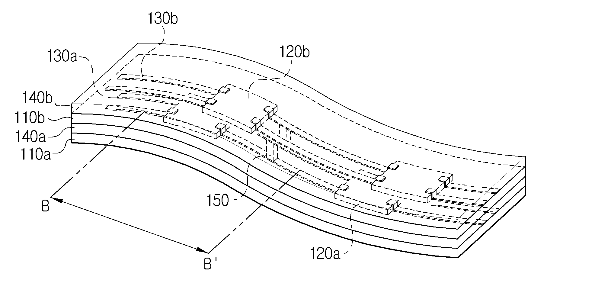
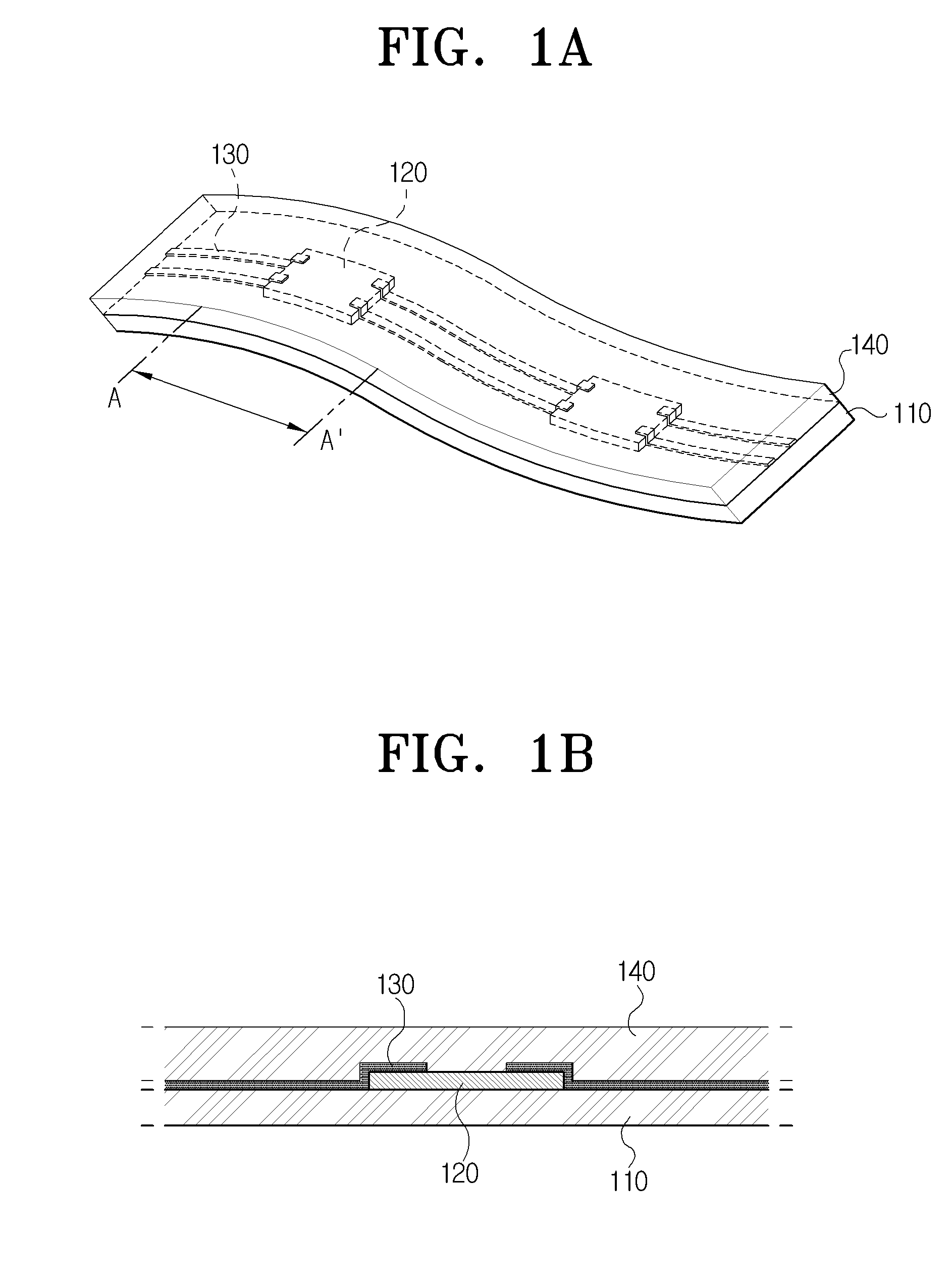
[0047]FIG. 1A is a perspective view is a flexible device in accordance with one exemplary embodiment of the present invention, and FIG. 1B is a cross-sectional view taken along an electrical interconnection 130 within an A-A′ range of the flexible device shown in FIG. 1A. Referring to FIGS. 1A and 1B, the present flexible device has a first flexible substrate 110, a second flexible substrate 140, an active element 120, and an electrical interconnection 130. The active element 120 is attached on the first flexible substrate 110 and the electrical interconnection 130 is formed thereon, and the second flexible substrate 140 is deposited on the active element 120 and the electrical interconn...


PUM


Abstract

A flexible device, a flexible pressure sensor, and a fabrication method thereof. The present flexible device includes: a first flexible substrate formed of a flexible material to have a flexibility; an active element formed to have a predetermined thickness and a flexibility, and being attached on the first flexible substrate; and a second flexible substrate formed of a flexible material to have a flexibility, and being deposited on the active element. The flexible device and the flexible pressure sensor have a high flexibility, so that they may be applied for a medical treatment such as implantation to a living body, a human body and so forth. In addition, the flexible device has a high flexibility, so that it may be inserted to a curved surface, which contributes to remove the limit of space where the semiconductor package device may be inserted.

Description

CROSS-REFERENCE TO RELATED APPLICATIONS[0001]This is a Divisional Application of U.S. application Ser. No. 11 / 221,935 filed Sep. 9, 2005, which claims priority under 35 U.S.C. § 119 from Korean Patent Application No. 2004-72630, filed on Sep. 10, 2004. The entire disclosure of the prior applications are incorporated herein by reference in their entirety.BACKGROUND OF THE INVENTION[0002]1. Field of the Invention[0003]The present invention relates to a semiconductor package device and a method of fabricating the same and, in particular, to a semiconductor package device in which a semiconductor device fabricated on a wafer is embedded and a method of fabricating the same.[0004]2. Description of the Related Art[0005]Semiconductor devices (e.g. chips) fabricated on a wafer are electrical devices, however, they may be not directly used by users and are apt to be broken. Accordingly, in order to use the semiconductor devices, they must be subjected to a packaging process for protection. T...

Claims


Application Information

Patent Timeline
Patent Type & Authority Applications(United States)
IPC IPC(8): H05K7/06
CPCG01L19/146H01L23/5387H01L2924/10253H01L23/5389H01L24/24H01L2224/24051H01L2924/01002H01L2924/01029H01L2924/01033H01L2924/01079H01L2924/01082H01L2924/14H01L2924/19041H01L2924/30105H01L2924/30107H05K1/185H05K1/189H01L2924/01005H01L2924/01006H01L2924/00H01L21/60
Inventor SHIN, KYU-HOMOON, CHANG-YOULKIM, YONG-JUN
Owner SAMSUNG ELECTRONICS CO LTD
Why Eureka
Try Eureka