Manufacturing method of display device

Active Publication Date: 2009-11-05
PANASONIC LIQUID CRYSTAL DISPLAY CO LTD +1
View PDF3 Cites 17 Cited by
  • Summary
  • Abstract
  • Description
  • Claims
  • Application Information

AI Technical Summary

Benefits of technology

[0029]According to the present invention, the portion of the first substrate which faces the terminal portion in an opposed manner can be cut without damaging the terminal portion of the second substrate and hence, there is no possibility that the terminal portion is damaged whereby it is possible to prevent the terminal portion from being damaged. Accordingly, the present invention can acqu

Problems solved by technology

However, when the above-mentioned terminal portion is cut, that is, when only the opposedly-facing CF board is cut, there has been a drawback that term

Method used


Image

  • Manufacturing method of display device
  • Manufacturing method of display device
  • Manufacturing method of display device

Examples


embodiment 1

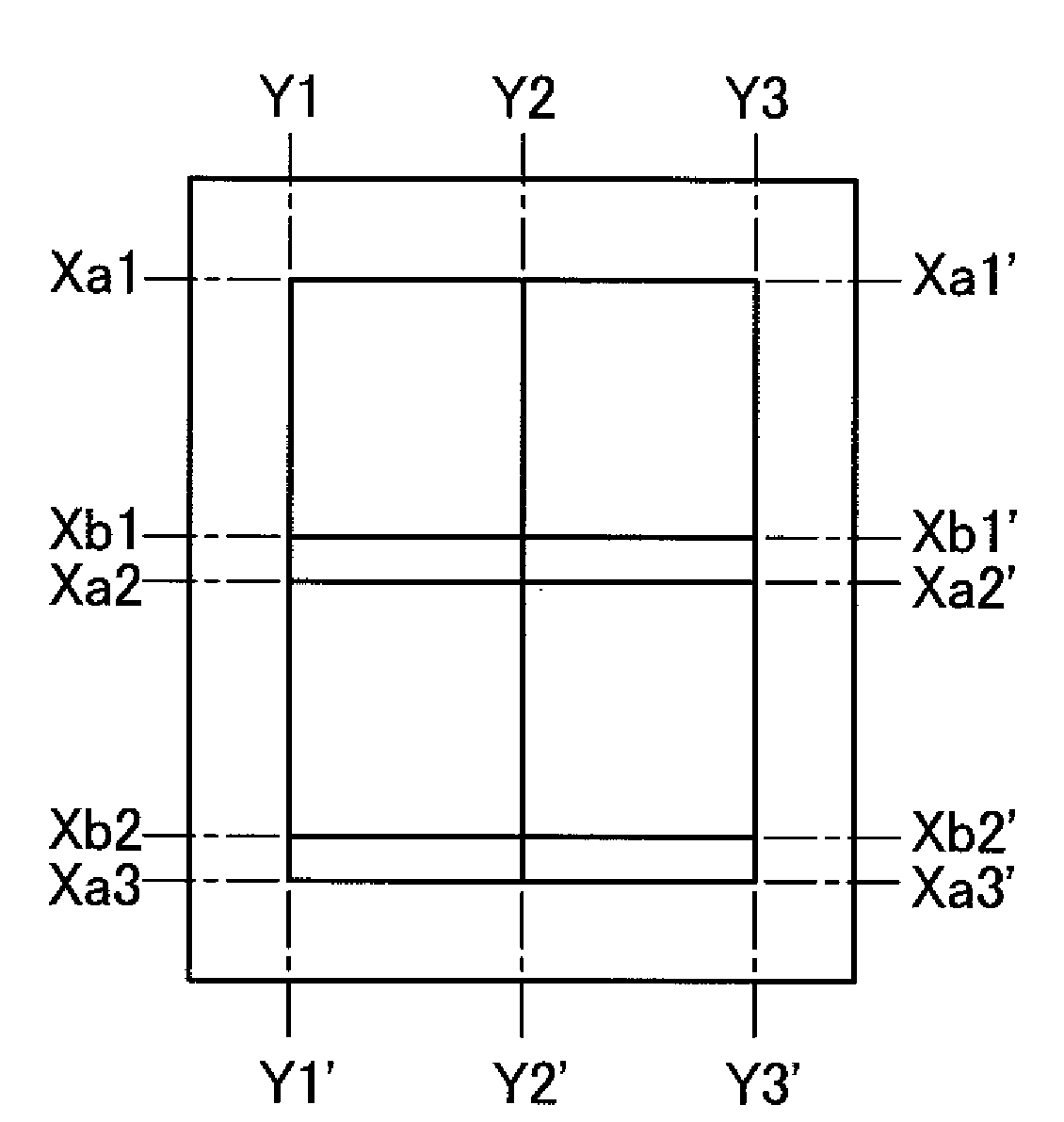
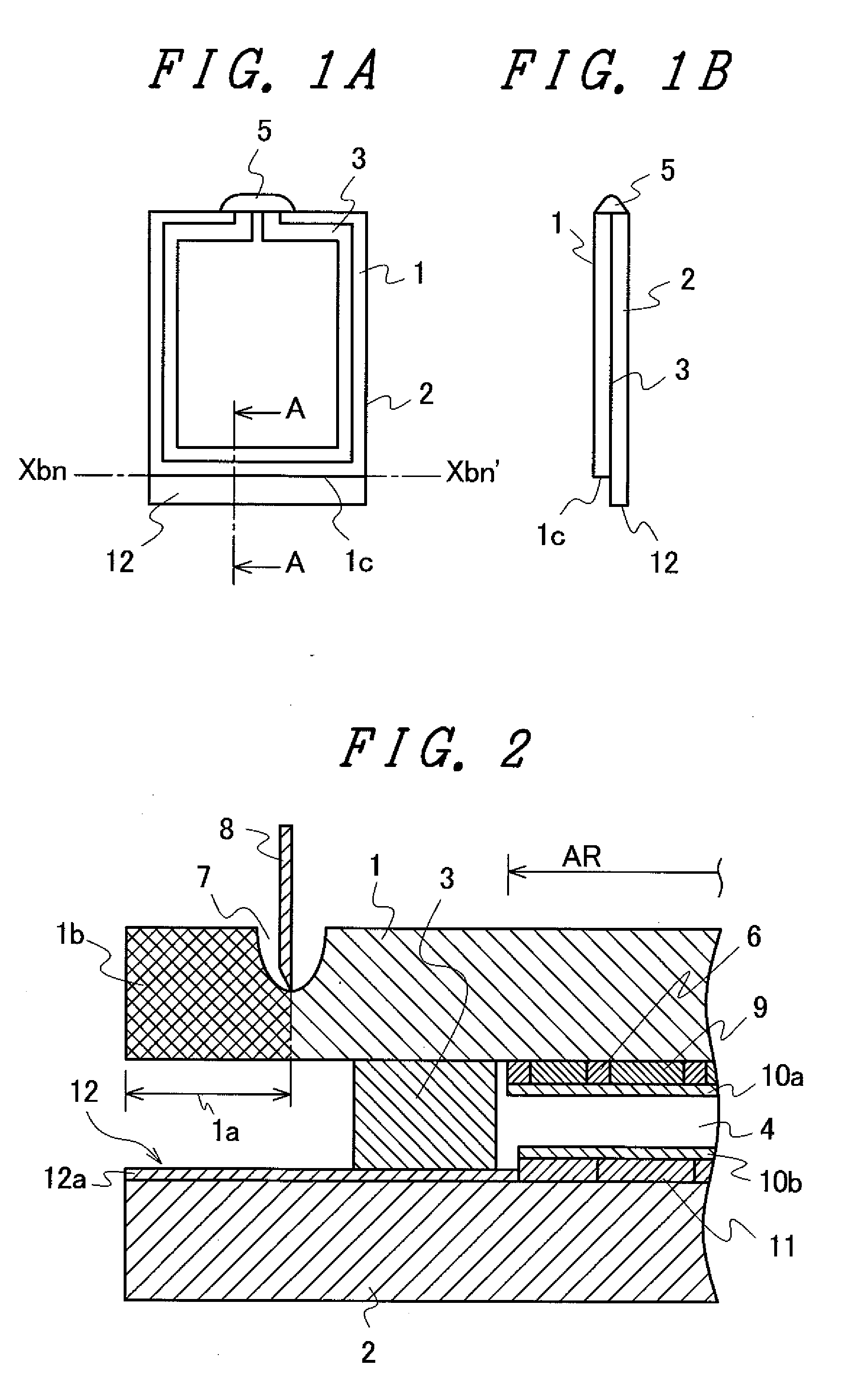
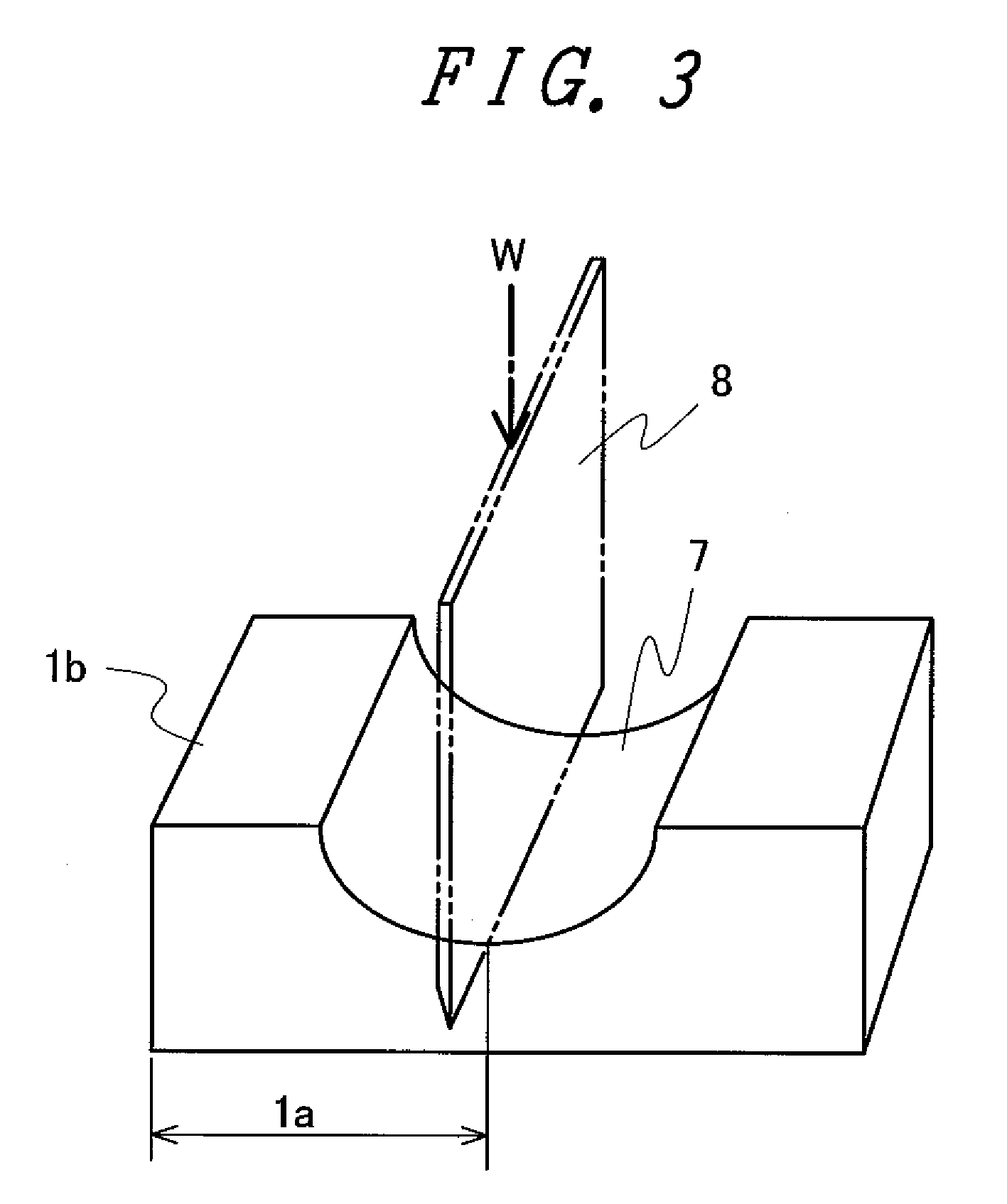
[0044]FIG. 1A and FIG. 1B are schematic views showing the constitution of a liquid crystal display panel for explaining a manufacturing method of a liquid crystal display device as one embodiment of a manufacturing method of a display device according to the present invention, wherein FIG. 1A is a top plan view of the liquid crystal display panel, and FIG. 1B is a side view of the liquid crystal display panel. Further, FIG. 2 is an enlarged cross-sectional view taken along a line A-A in FIG. 1A.

[0045]In FIG. 1A and FIG. 1B, the liquid crystal display panel is configured as follows. A first substrate 1 (also referred to as a color filter substrate 1 or a CF substrate 1) which is formed of a light transmitting plastic substrate having a thickness of approximately 0.2 mm and a second substrate 2 (also referred to as a thin film transistor substrate 2 or a TFT substrate 2) which is formed of a light transmitting plastic substrate on which a plurality of lines and a plurality of terminal...

embodiment 2

[0070]FIG. 9 is a cross-sectional view of an essential part of a cut portion for explaining another embodiment of the manufacturing method of the display device according to the present invention by taking a liquid crystal display device as an example. In FIG. 9, parts identical with the parts shown in the above-mentioned drawings are given same numerals and their explanation is omitted.

[0071]In the liquid crystal display device of the embodiment 1, the explanation is made with respect to the case in which the first substrate 1 is formed of a single-layered substrate. However, this embodiment is directed to the a case in which the first substrate 1 is formed of a multi-layered substrate where a polarizer layer and an optical film having phase-difference property are formed on a liquid crystal display panel in a stacked manner. The explanation of this embodiment is made in conjunction with FIG. 9.

[0072]In FIG. 9, in the liquid crystal display device of this embodiment, a first light ...

embodiment 3

[0076]FIG. 10 is a view for explaining still another embodiment of the manufacturing method of the display device according to the present invention. In FIG. 10, parts identical with the parts shown in the above-mentioned drawings are given same numerals and their explanation is omitted. In FIG. 10, with respect to the broken portion of the liquid crystal display panel shown in FIG. 5, a resin 13 is applied to the broken portion by coating for protecting the broken portion. That is, the resin 13 covers the substantially whole surface of the groove 7 formed in the first substrate 1 at a position where the groove 7 faces the terminal portion 12 in an opposed manner, the mark 8a having an acute angle formed by the cutter 8, and the broken portion of the substrate broken surface 1c. Further, the resin 13 is filled into a gap defined between the first substrate 1 and the second substrate 2 so that the resin 13 is brought into contact with the sealing material 3.

[0077]The resin 13 may be ...


PUM


Abstract

A liquid crystal display device having high quality and high reliability is manufactured by preventing the occurrence of damages on a terminal portion due to the radiation of laser beams in cutting a substrate of the display device which is formed using a plastic substrate by the radiation of laser beams. A first substrate has a cutting line at a position which faces a terminal portion of a second substrate. In cutting the first substrate along the cutting line, laser beams are radiated to the first substrate along the cutting line so as to form a groove having a predetermined depth in the first substrate. Then, a load is applied to the first substrate along the groove so as to cut the first substrate.

Description

[0001]The present application claims priority from Japanese application JP2008-118105 filed on Apr. 30, 2008, the content of which is hereby incorporated by reference into this application.BACKGROUND OF THE INVENTION[0002]1. Field of the Invention[0003]The present invention relates to a manufacturing method of a display device, and more particularly to a manufacturing method of a display device using a display panel which is formed such that a plurality of display panels is formed on a large-sized mother board and, thereafter, the mother board is divided into individual display panels by cutting. The present invention, more particularly, relates to a manufacturing method of a liquid crystal display device.[0004]2. Description of the Related Art[0005]Recently, a demand for making a display device flexible has been increasing. The development of a plastic substrate made of a flexible base material which can cope with such a demand has been in progress. In the manufacture of an existin...

Claims


Application Information

Patent Timeline
IPC IPC(8): H01L21/84H01L21/301B23K26/38G02F1/13G09F9/00
CPCG02F1/133351
Inventor OKAMOTO, MASATAKAMATSUYAMA, SHIGERU
Owner PANASONIC LIQUID CRYSTAL DISPLAY CO LTD
Why Eureka
Try Eureka