

Semiconductor device
- Summary
- Abstract
- Description
- Claims
- Application Information
AI Technical Summary
Benefits of technology
Problems solved by technology
Method used
Image

Examples
Embodiment Construction
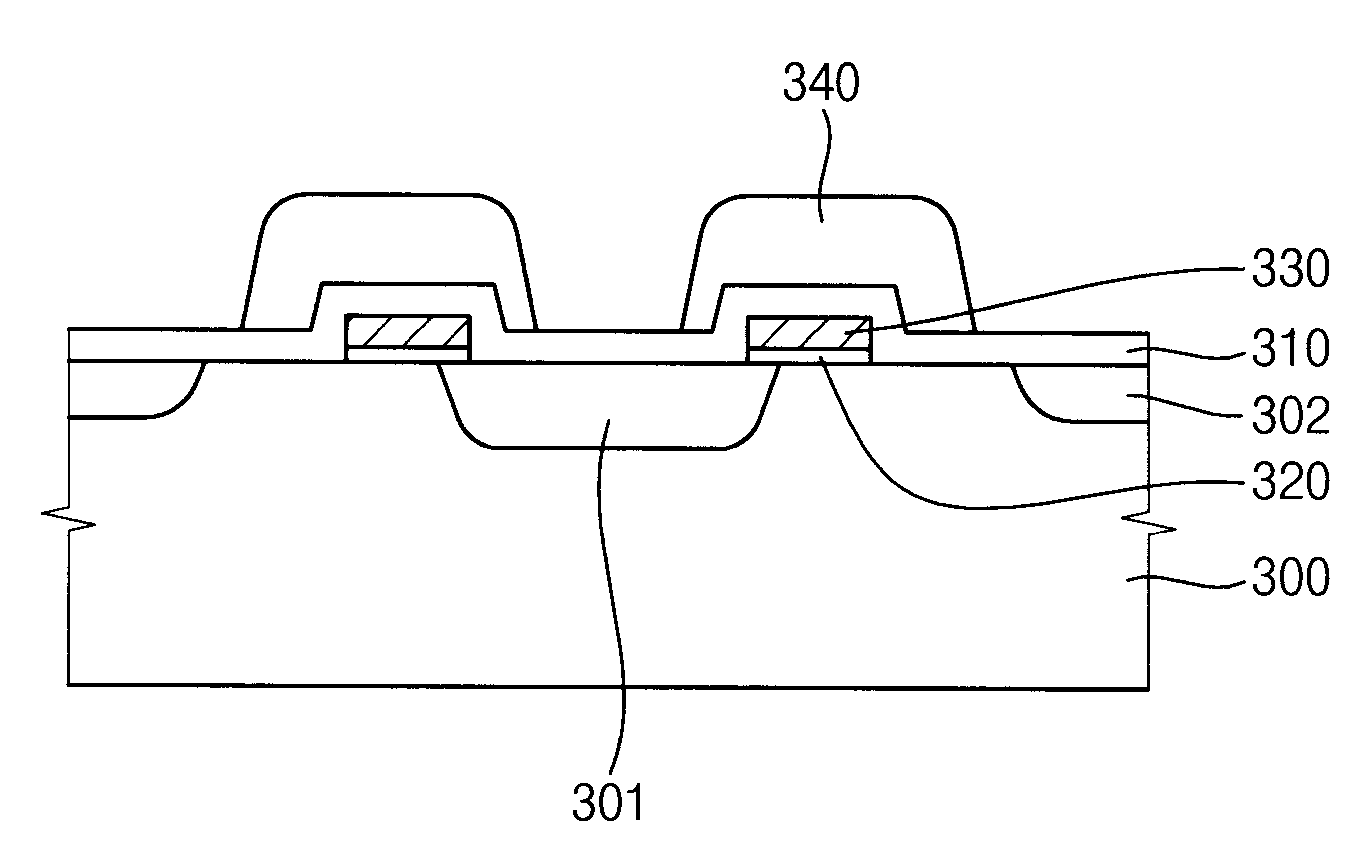
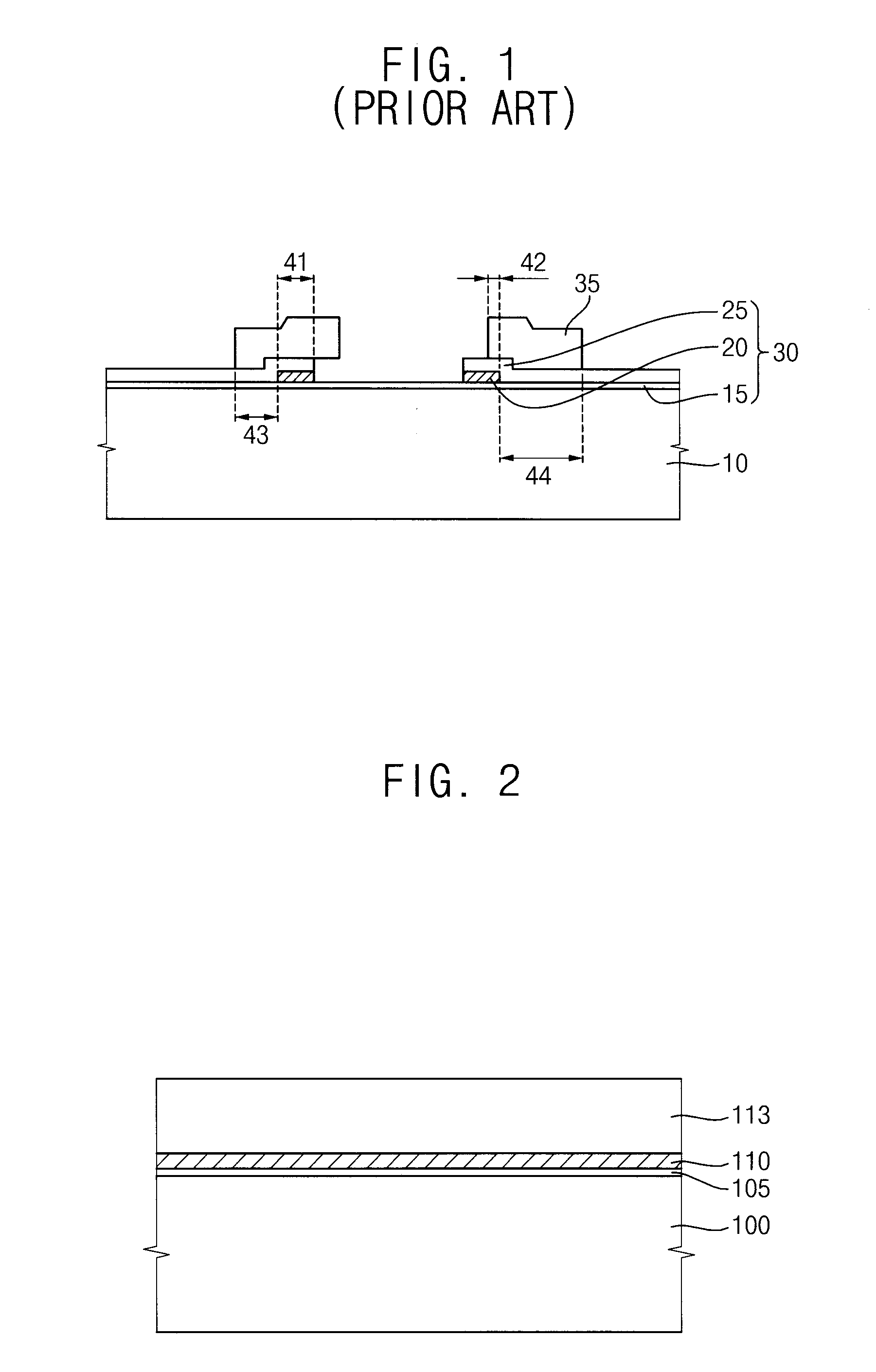
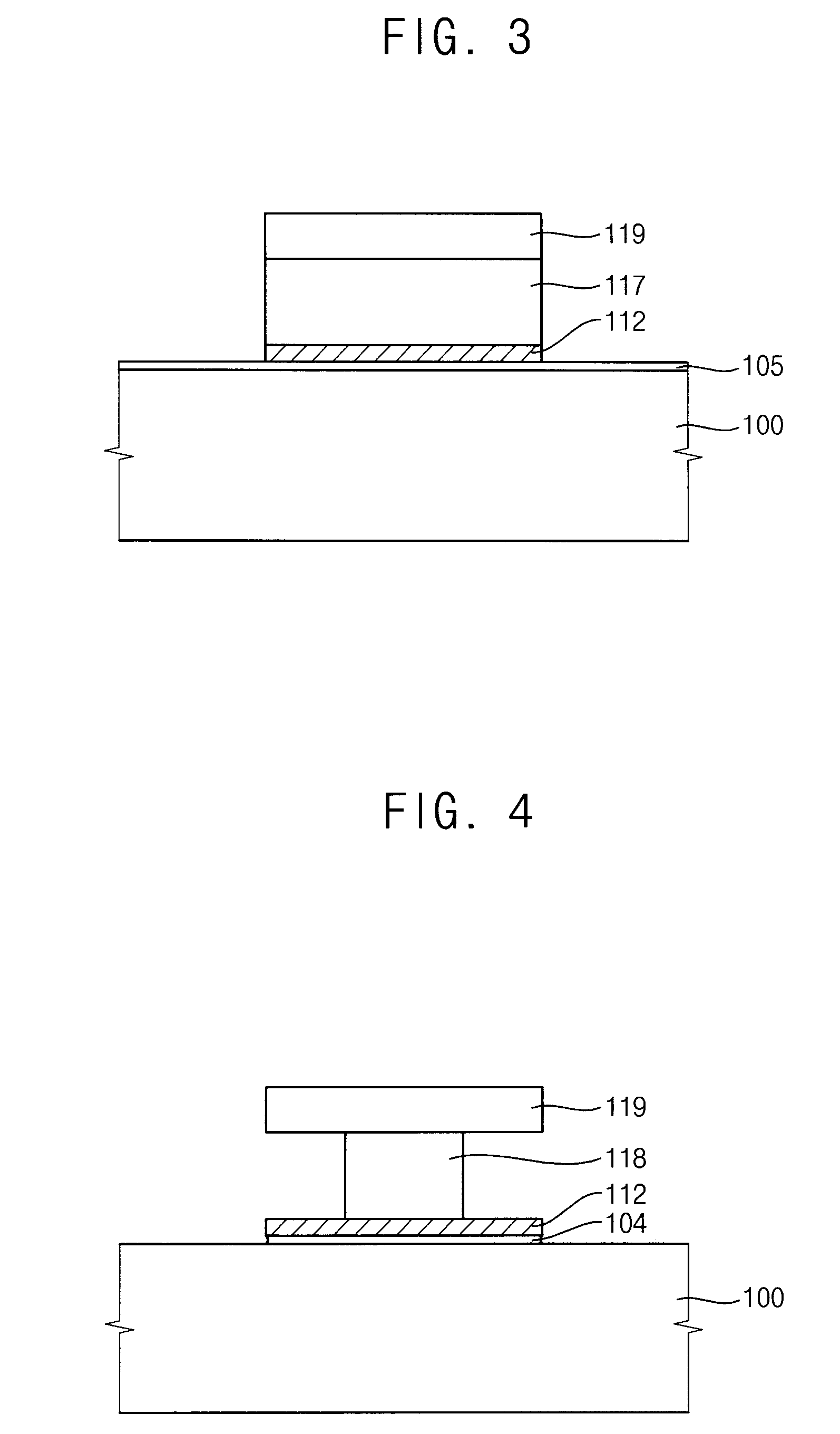
[0028]The present invention will be described more fully hereinafter with reference to the accompanying drawings. Those numerals which are the same in different drawings designate like elements. Also, in the drawings, the sizes and relative sizes of layers and regions may be exaggerated for clarity.
[0029]Furthermore, when an element or layer is referred to as being disposed “on,” another element or layer, such a description includes the case in which the element or layer is disposed directly on the other element or layer as well as the case in which another element(s) or layer(s) is / are present therebetween. Likewise, when an element is referred to as being “connected to” or “coupled to” another element, such a description includes the case in which the element is directly connected or coupled to the other element as well as the case in which another element(s) is / are coupled or connected therebetween.
[0030]Terms, such as “beneath,”“below,”“lower,”“above,”“upper” and the like, may b...
PUM
 Abstract
Description
Claims
Application Information