Wiring board

a wiring layer and wire technology, applied in the direction of printed circuit manufacturing, semiconductor/solid-state device details, printed circuit aspects, etc., can solve the problems of lowering the reliability of connection between the chip and the package, disconnecting the electrode terminals of the chip and the wiring layer from each other, and the resin fillet of the underfill resin b>60/b> (portion surrounded by a broken line df) is not sufficiently formed, so as to improve the flow performance of resin

Active Publication Date: 2009-11-19
SHINKO ELECTRIC IND CO LTD
View PDF4 Cites 8 Cited by
  • Summary
  • Abstract
  • Description
  • Claims
  • Application Information

AI Technical Summary

Benefits of technology

[0021]An object of the present invention is to provide a wiring board capable of allowing a reliable formation of resin fillet by improving flow performance of resin in a corner portion of an object to be mounted such as a semiconductor chip without causing generation of void within resin when the resin is filled into a gap between the object and the wiring board in the state where the object is mounted.

Problems solved by technology

However, where the edge of the opening portion is positioned inside the mounting area of the chip on the wiring board, the following problems occur.
When the void is formed, the connection reliability between the chip and package is lowered because sufficient bonding strength cannot be obtained.
In addition, the air inside the void expands due to heat processing after the filling of the resin, which may generate a crack in the underfill resin, and in some cases, may disconnect the electrode terminals of the chip and the wiring layer from each other.
However, there is a disadvantage in that a fillet of the underfill resin 60 (portion surrounded by a broken line DF) is not sufficiently formed as schematically illustrated in the cross-sectional view of FIG. 6B (cross-sectional view of the vicinity of the corner portion R4 in the opening portion 48).
However, the presence of such area depreciates the appearance of the package.
Namely, the insufficient fillet of the underfill resin 60 adversely affects outer appearance.
In this type of package, when the corner portion is not sufficiently filled with the resin as exemplified in FIG. 6, there occurs a problem in terms of insulation properties because the wiring or the like is exposed.
Specifically, taking into consideration the case where: first, a semiconductor chip is mounted on a lower package (wiring board) by flip chip mounting; then, bumps formed on a mounting surface side of an upper package are bonded, via solder or the like, to conductor portions (pad portions) formed in a peripheral region of the chip on the lower package; and an underfill resin is filled between the upper and lower packages, the above problem may possibly occur likewise.

Method used


Image

  • Wiring board
  • Wiring board
  • Wiring board

Examples


Embodiment Construction

[0032]Description is given below of preferred embodiments of the present invention with reference to the accompanying drawings.

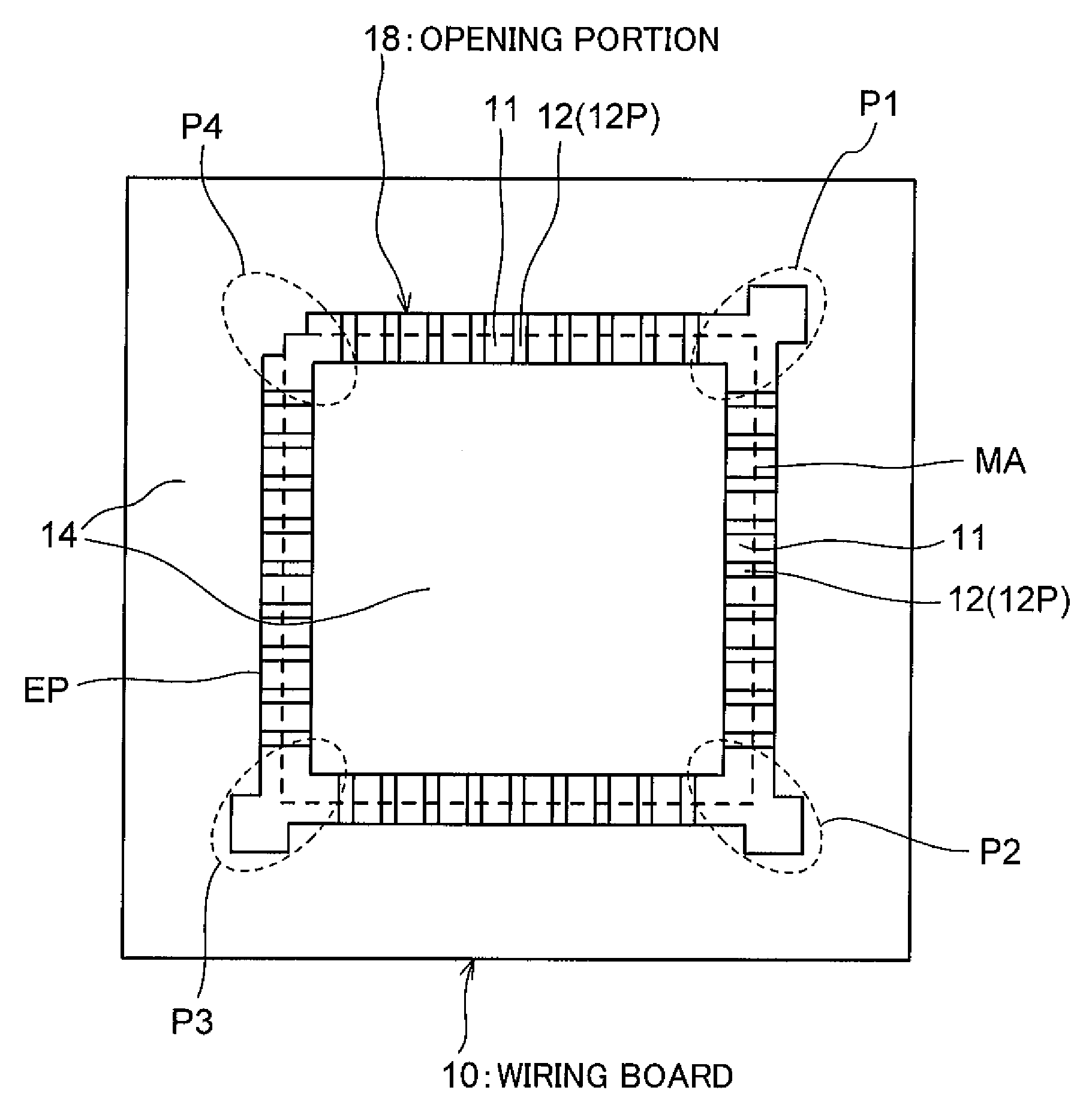
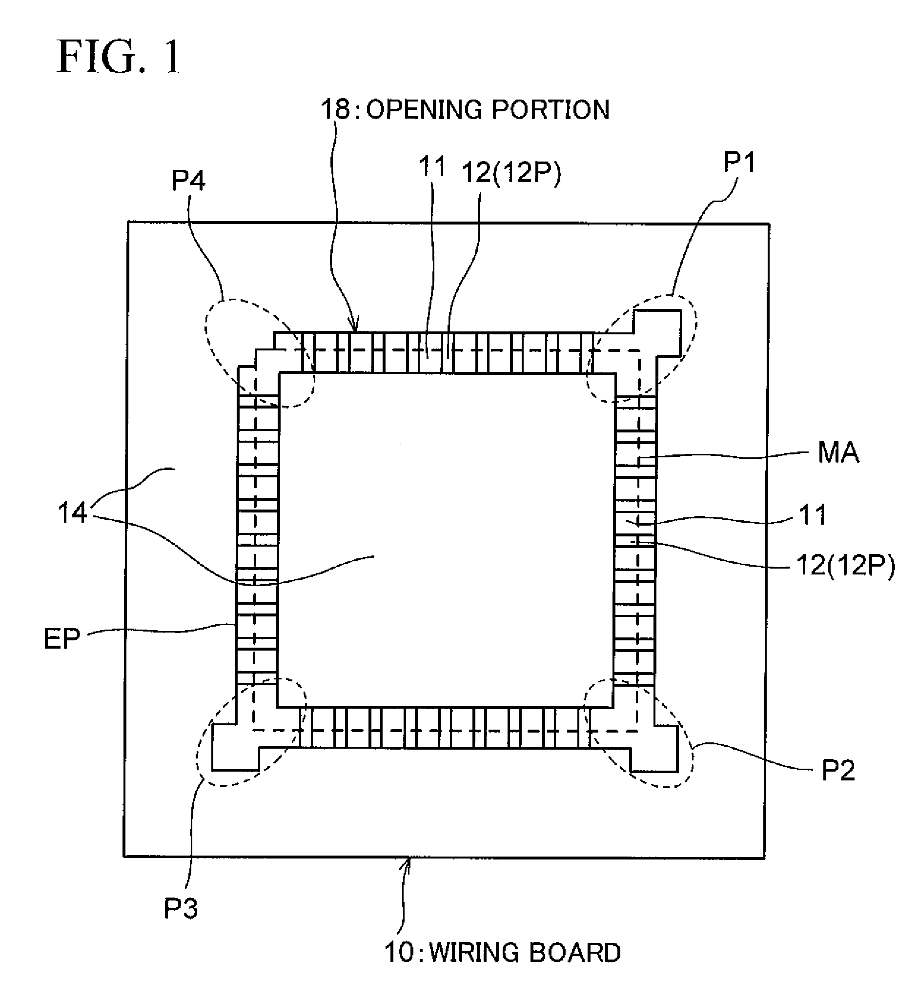
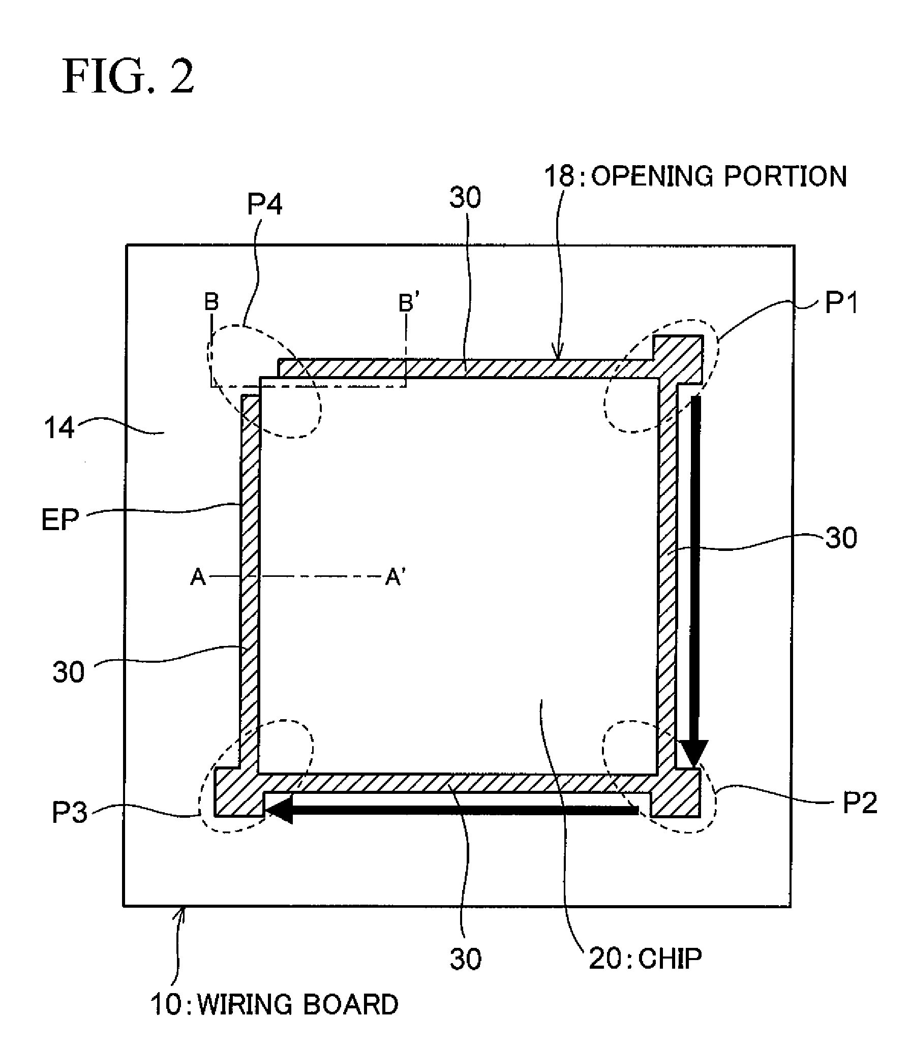
[0033]FIG. 1 shows in a plan view, the configuration of a wiring board (package) for flip chip mounting according to one embodiment of the present invention. FIG. 2 shows in a plan view, a state where a gap between a semiconductor chip and the wiring board of FIG. 1 is filled with resin when the semiconductor chip is mounted. FIGS. 3A and 3B show a vertical cross-sectional structure of the vicinity of an opening portion of the solder resist layer in the configuration of FIG. 2. Specifically, FIG. 3A shows a cross-sectional structure when viewed along A-A′ line of FIG. 2 (the vicinity of a portion along a side of the chip in the opening portion), and FIG. 3B shows a cross-sectional structure when viewed along B-B′ line of FIG. 2 (the vicinity of a corner portion in the opening portion).

[0034]First, referring to FIGS. 3A and 3B, the wiring board (package) 10 a...


PUM


Abstract

A wiring board between which and a chip to be mounted a resin is filled includes: a substrate body on which a conductor portion to be connected to an electrode terminal of the chip is formed; and an insulating protection film formed on the substrate body and having an opening portion formed therein to expose the conductor portion. The opening portion is formed in such a manner that the edge thereof is positioned along and outside the outer shape of the chip except for a specific corner portion, and that the edge in the specific corner portion is positioned on a side of or inside the outer shape of the chip.

Description

CROSS-REFERENCE TO RELATED APPLICATIONS[0001]This application is based on and claims priority of Japanese Patent Application No. 2008-128194 filed on May 15, 2008, the entire contents of which are incorporated herein by reference.BACKGROUND OF THE INVENTION[0002](a) Field of the Invention[0003]The present invention relates to a wiring board for use in mounting thereon an object to be mounted such as a semiconductor chip or a semiconductor device. More particularly, the present invention relates to a wiring board having a structure in which resin is filled between a semiconductor chip or the like and the wiring board when the semiconductor chip or the like is mounted thereon by flip chip bonding.[0004]Note that, the “wiring board” is hereinafter also referred to as a “semiconductor package” or merely a “package” for the sake of convenience, because it has the function of mounting thereon a semiconductor chip or the like.[0005](b) Description of the Related Art[0006]In recent years, s...

Claims


Application Information

Patent Timeline
Patent Type & Authority Applications(United States)
IPC IPC(8): H05K1/11
CPCH01L23/49822H01L2224/81193H01L24/16H01L2224/13099H01L2224/16225H01L2224/27013H01L2224/32225H01L2224/73204H01L2224/83051H01L2224/83385H01L2924/01002H01L2924/01005H01L2924/01013H01L2924/01015H01L2924/01029H01L2924/01033H01L2924/01047H01L2924/0105H01L2924/01078H01L2924/01079H01L2924/01082H01L2924/01322H01L2924/14H01L2924/15311H05K3/305H05K3/3452H05K2201/0989H05K2201/10674H05K2201/10977H01L24/32H01L2924/01006H01L2924/0132H01L23/49838H01L2224/26175H01L2224/29111H01L2924/1579H01L2224/2919H01L2924/0133H01L2924/00012H01L2924/3512H01L2924/00H01L2924/0665H01L2224/05571H01L2224/05573H01L2924/00014H01L2924/15787H01L2224/05599
Inventor OZAWA, TAKASHI
Owner SHINKO ELECTRIC IND CO LTD
Why Eureka
Try Eureka