Transparent conductive film, electrode sheet for use in touch panel, and touch panel
a technology of transparent conductive film and electrode sheet, which is applied in the direction of conductive layer on the insulating support, instruments, transportation and packaging, etc., can solve the problems of inability to use for certain purposes, low flexibility or workability, and so as to prevent the formation of newton's rings
- Summary
- Abstract
- Description
- Claims
- Application Information
AI Technical Summary
Benefits of technology
Problems solved by technology
Method used
Image
Examples
example 1
Preparation of Coating Liquid
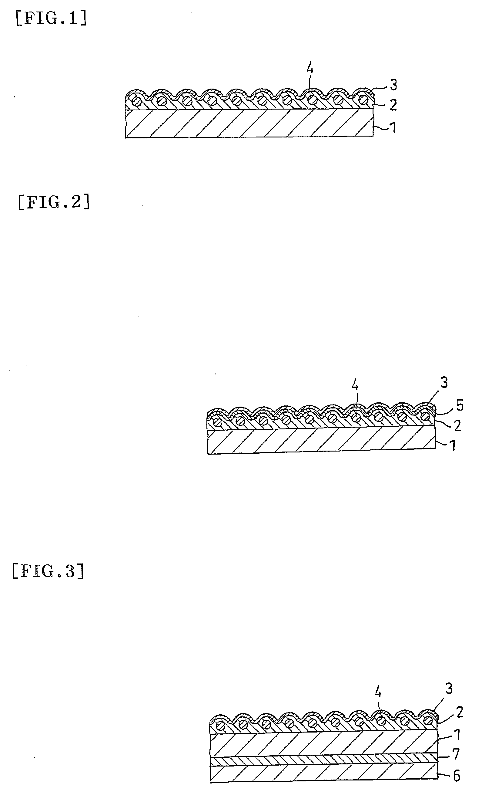
[0084]The fine particles used was a mixture of 0.5 parts of a monodisperse filler with an average particle size of 2.2 μm (material, crosslinked acrylic resin; particle size standard deviation, 0.22 μm; product grade, MX-type manufactured by Soken Chemical & Engineering Co., Ltd.) and 0.1 parts of a monodisperse filler with an average particle size of 3 μm (material, crosslinked acrylic resin; particle size standard deviation, 0.3 μm; product grade, MX-type manufactured by Soken Chemical & Engineering Co., Ltd.). A solution was prepared by mixing the fine particle mixture, 100 parts of an ultraviolet curable resin (acrylic-urethane resin Unidic 17-806 (trade name) manufactured by Dainippon Ink and Chemicals, Incorporated), 5 parts of a photopolymerization initiator (Irgacure 184 (trade name) manufactured by Ciba Specialty Chemicals Inc.), and a solvent (toluene) in such an amount that the solution had a solids content of 50% by weight.
Preparation of Resi...
example 2
[0087]The coating liquid prepared in Example 1 was used. A resin layer was formed using the process of Example 1, except that the thickness of the coating for the resin layer was changed to 1.4 μm in the process of forming the resin layer. A transparent conductive film was then prepared using the process of Example 1.
example 3
[0088]The coating liquid prepared in Example 1 was used. A resin layer was formed using the process of Example 1, except that the thickness of the coating for the resin layer was changed to 1.8 μm in the process of forming the resin layer. A transparent conductive film was then prepared using the process of Example 1.
PUM
| Property | Measurement | Unit |
|---|---|---|
| height | aaaaa | aaaaa |
| height | aaaaa | aaaaa |
| Ra | aaaaa | aaaaa |
Abstract
Description
Claims
Application Information


