Electronic skin having uniform gray scale reflectivity

a technology of gray scale reflectivity and electrooptic devices, applied in optics, non-linear optics, instruments, etc., can solve the problems of reducing the sensitivity of gray scale to display imperfections, affecting the sensitivity of prior art gray scale drive schemes, and displaying imperfections in the conductive layer forming electrodes. , to achieve the effect of avoiding gray scale discontinuities, and reducing the sensitivity of gray levels

Inactive Publication Date: 2009-11-19
MANNING VENTURES
View PDF23 Cites 70 Cited by
  • Summary
  • Abstract
  • Description
  • Claims
  • Application Information

AI Technical Summary

Benefits of technology

[0015]In this disclosure, a new drive scheme is described for cholesteric liquid crystal displays. The drive scheme is applicable to glass- or plastic-based displays. Driving the display with the new scheme minimizes the sensitivity of the gray levels to display imperfections and reduces the need for further improvements in display manufacturing processes.
[0016]The electronic skin avoids gray scale discontinuities caused by imperfections in the display that may arise by: imperfections in the electrodes; non-uniform cell gap; non-uniform polymer dispersions; non uniform structure of the cholesteric liquid crystal such as caused by non-uniform surface induced alignment or other means. Reduction voltage pulses of narrow width are used to reduce the sensitivity of gray levels so that imperfections in the display are not visible in the gray levels therefore providing a uniform reflective intensity of a Bragg reflective color. In prior art displays having a liquid crystal sandwiched between two substrates, cell gap is the measured distance between the substrates. Such prior art displays normally have electrodes patterned on the inside of each substrate in contact with the liquid crystal layer, the electrodes being extremely thin on the order of angstroms. Prior art substrates of liquid crystal displays are normally made of glass and are very thick in comparison to the very thin liquid crystal layer, which can be on the order of 10 microns or less in thickness. Ce

Problems solved by technology

Thus, the prior art gray scale drive scheme is sensitive to applied voltage and display imperfections.
These imperfections can be particularly troublesome in displays with plastic substrates and can be worse for displays of large area.

Method used


Image

  • Electronic skin having uniform gray scale reflectivity
  • Electronic skin having uniform gray scale reflectivity
  • Electronic skin having uniform gray scale reflectivity

Examples


example 1

[0064]Levels of gray are levels of brightness as they are reduced from the maximum brightness exhibited by the planar texture of a particular electronic skin. In order to demonstrate the difference between uniform and non-uniform levels of gray, a bistable cholesteric cell illustrated in FIG. 4 was constructed. The glass cell was constructed using two 5.5×5.5 inch glass substrates, each 0.55 mm thick with ITO transparent conductors. The glass substrates were of unpolished glass exhibiting an expected roughness and not a perfectly smooth surface. The cell gap spacing was set by the use of glass spacers with an average size of 9 microns. However, because of the roughness of the substrates the cell gap was expected to have imperfections in cell gap thickness by as much as 0.4 μm which is typical for the use of unpolished glass. The glass cell was filled with a cholesteric liquid crystal KLC-23, a Kent Displays, Inc. proprietary mixture of a nematic liquid crystal with a large dielectri...

example 2

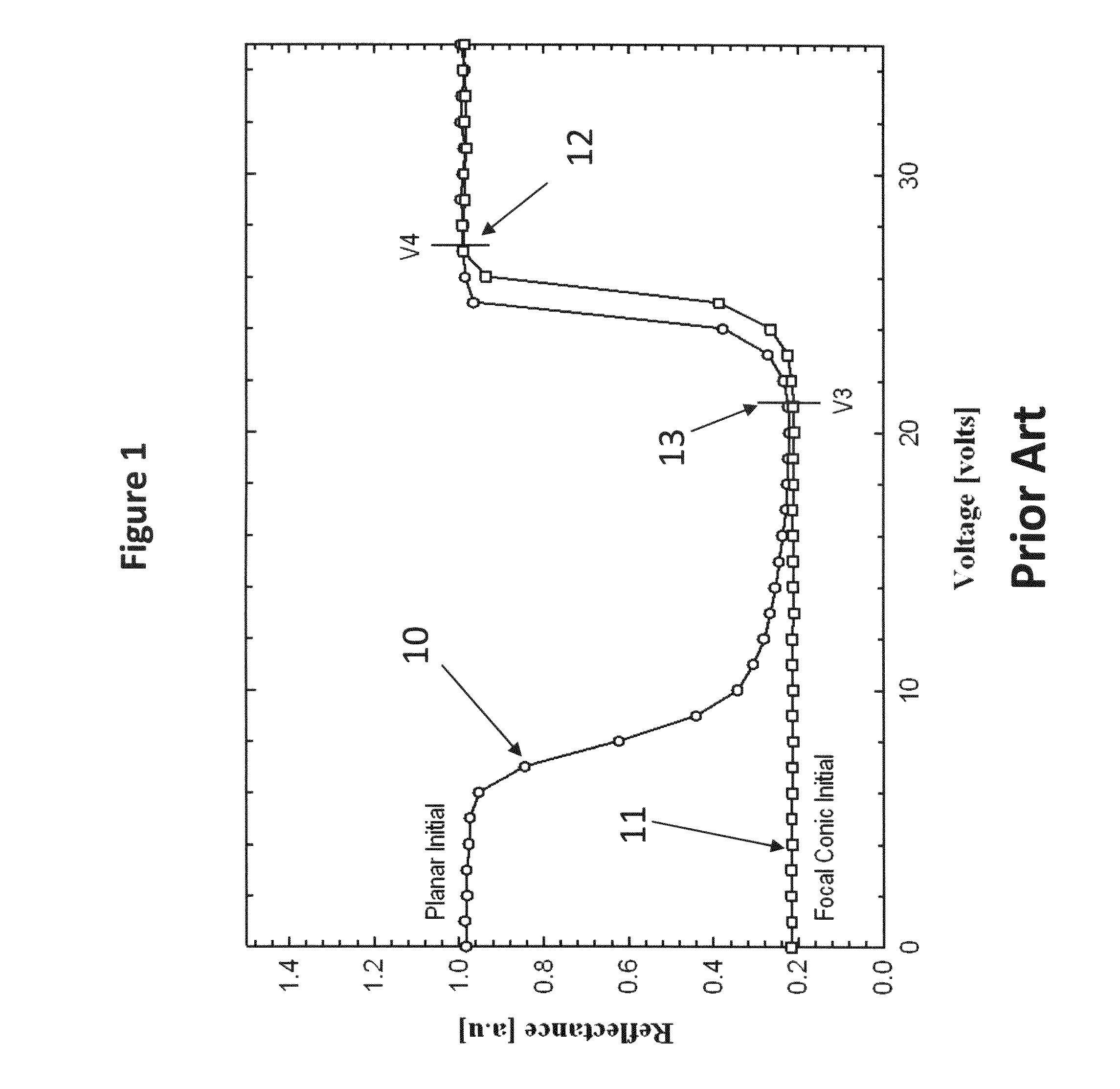
[0066]Electrooptic response curves which are a plot of the reflectance of the cell versus the rms voltage of a pulse are experimentally achieved for a bistable cholesteric cell for various pulse widths as shown in FIG. 6. While acquiring each of the data points, the cell was observed visually with the eye to determine if the cell exhibited a uniform or non-uniform gray level. The glass cell was constructed using two 2×2 inch glass substrates, each 1.0 mm thick with ITO transparent conductors. The glass substrates were of unpolished glass exhibiting an expected roughness and not a perfectly smooth surface. The cell gap spacing was set by the use of glass spacers with an average size of 5.0 microns. However, because of the roughness of the substrates the cell gap was expected to have imperfections in cell gap thickness by as much as 0.4 μm expected for unpolished glass. The glass cell was filled with the same cholesteric liquid crystal KLC-23, (Kent Displays, Inc.) as used in Example ...

example 3

[0068]In this example, while not wanting to be bound by theory, we estimated the variation of the cell gap distance from the data of FIG. 6 based on the assumption it is due to the variation in the surface roughness of the unpolished glass surface of the substrates from which the cell was formed. The premise of this example is that the slopes of the curves in FIG. 6 determine the sensitivity of gray levels to the imperfections in the bistable cholesteric cell. This is supported by the observation that the solid data points (points exhibiting uniform gray levels) all terminate on the left side of each curve at about the same slope. This value is given by the ratio (ΔR / ΔV)max where ΔR is the change in Reflectance and ΔV is the corresponding change in Voltage at a point on the curve. From the curves it is found that (ΔR / ΔV)max≈0.02. If the non-uniformity is due to variations in cell gap then one obtains:

(ΔR / ΔV)max=(ΔR) / E(Δd)≈0.02.  Eq. 1

[0069]Where E is the electric field and Δd is the...


PUM

PropertyMeasurementUnit
Electrical conductivityaaaaaaaaaa
Coloraaaaaaaaaa
Flexibilityaaaaaaaaaa

Abstract

The invention features electronic skin including an active layer formed of bistable cholesteric liquid crystal material and articles comprising the skin, the electronic skin having uniform gray scale reflectivity. Also featured is method for producing suitable reduction pulses that will provide a display (e.g., the electronic skin) with uniform gray scale reflectivity. Reduction pulses of narrow width are used to create uniform levels of gray in the electronic skin to overcome display imperfections that cause discontinuity in the gray scale reflectivity.

Description

FIELD OF THE INVENTION[0001]The invention pertains to gray scale of electro-optic devices and, in particular to achieving uniform gray scale of liquid crystal devices that are susceptible to gray scale discontinuities, therefore enabling electronic skins that can exhibit uniform tunable colors over a large area.BACKGROUND OF INVENTION[0002]Bistable cholesteric liquid crystal displays were introduced in the early 1990's (see U.S. Pat. Nos. 5,437,811 and 5,453,863). Their zero-power image retention and sunlight readability led to their integration into numerous signs and battery-powered applications as reviewed in “Cholesteric Liquid Crystals for Flexible Displays” in Flexible Flat Panel Displays, Ed. G. Crawford, (John Wiley & Sons, 2005) J. W. Doane and A. Khan, Chapter 17. The technology is best suited for reflective color images. In the cholesteric display technology, multiple-color and full-color displays are preferably produced by stacking multiple cholesteric liquid crystal lay...

Claims


Application Information

Patent Timeline
IPC IPC(8): G02F1/139G02F1/1334
CPCG02F1/1347G02F1/1391G02F1/13718
Inventor MARHEFKA, DUANE W.VENKATARAMAN, NITHYABARUA, SANKAR
Owner MANNING VENTURES
Why Eureka
Try Eureka