
Wiring substrate and method of manufacturing the same

a technology of wiring substrate and wiring layer, which is applied in the manufacture of cable/conductor, printed circuit, basic electric elements, etc., can solve the problems of pattern disappearance, large unevenness of the surface thereof, so as to reduce the surface roughness increase the adhesion of the insulating layer to the wiring layer, and reduce the effect of ra

Inactive Publication Date: 2009-11-26
SHINKO ELECTRIC IND CO LTD
View PDF8 Cites 41 Cited by
  • Summary
  • Abstract
  • Description
  • Claims
  • Application Information

AI Technical Summary

Benefits of technology

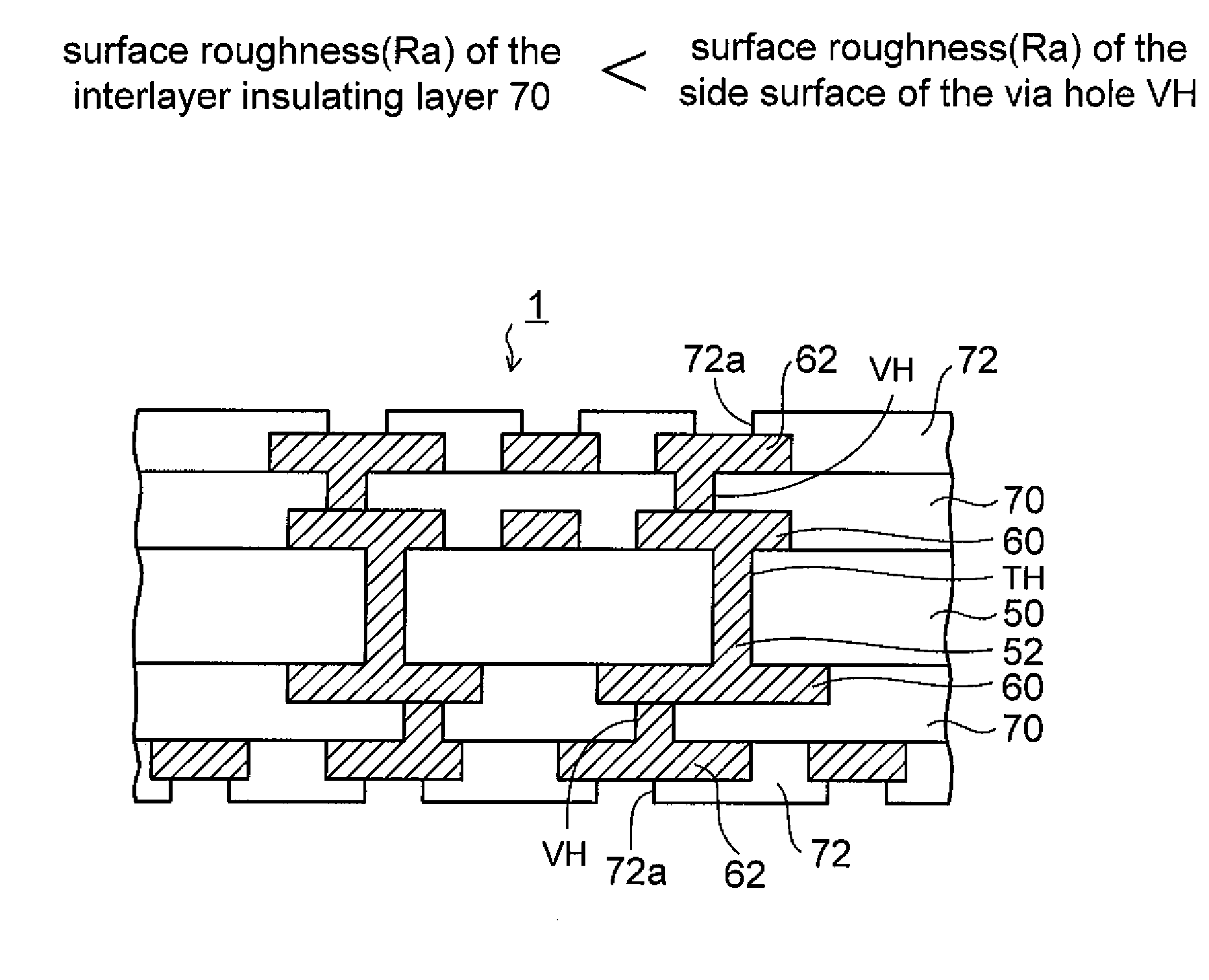
[0018]It is an object of the present invention to provide a wiring substrate and a method of manufacturing the same, capable of responding to miniaturization (line:space=15:15 μm or less) of a wiring layer, and also obtaining sufficient adhesion between the wiring layer and an underlying insulating layer.

Problems solved by technology

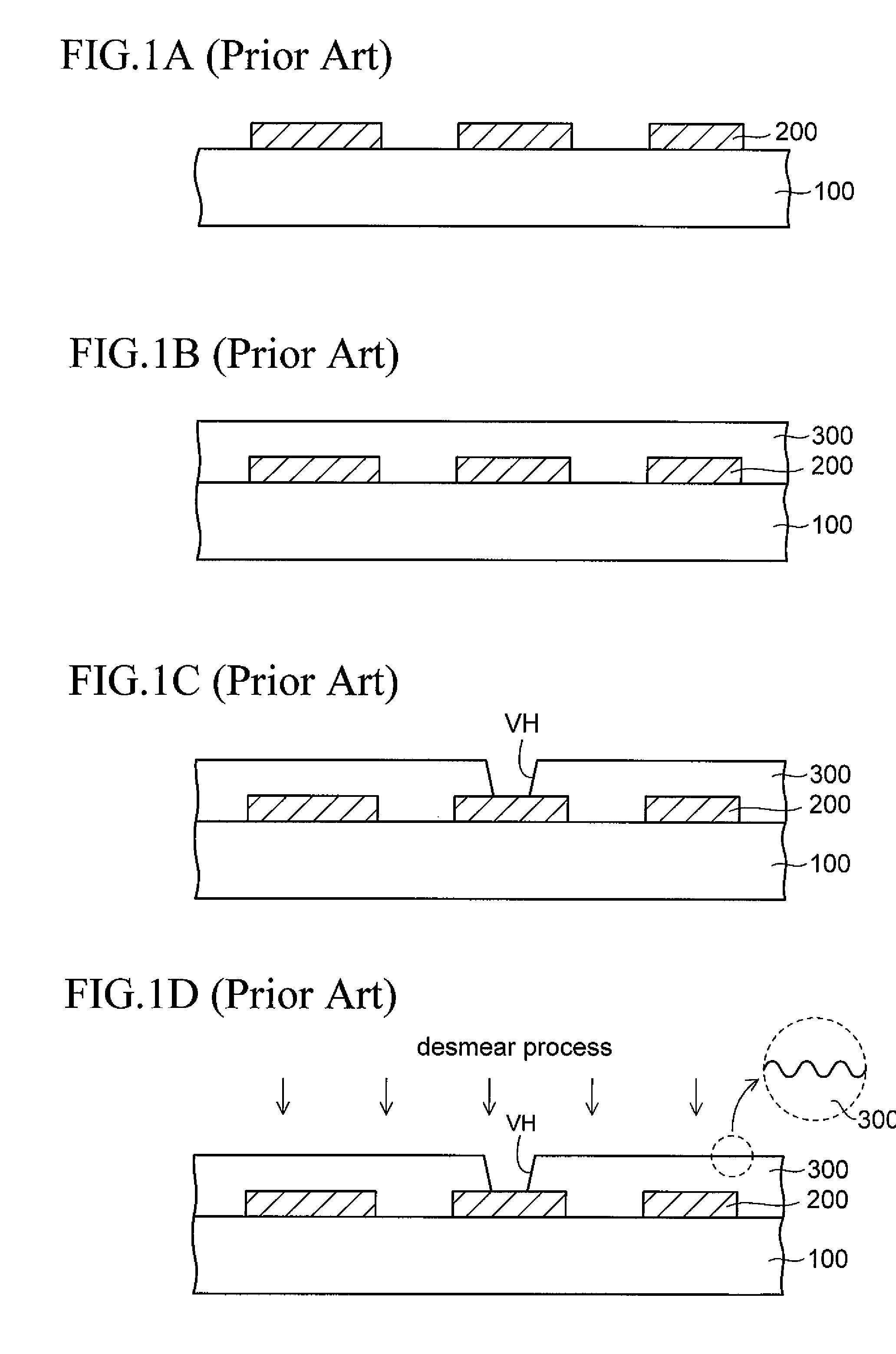
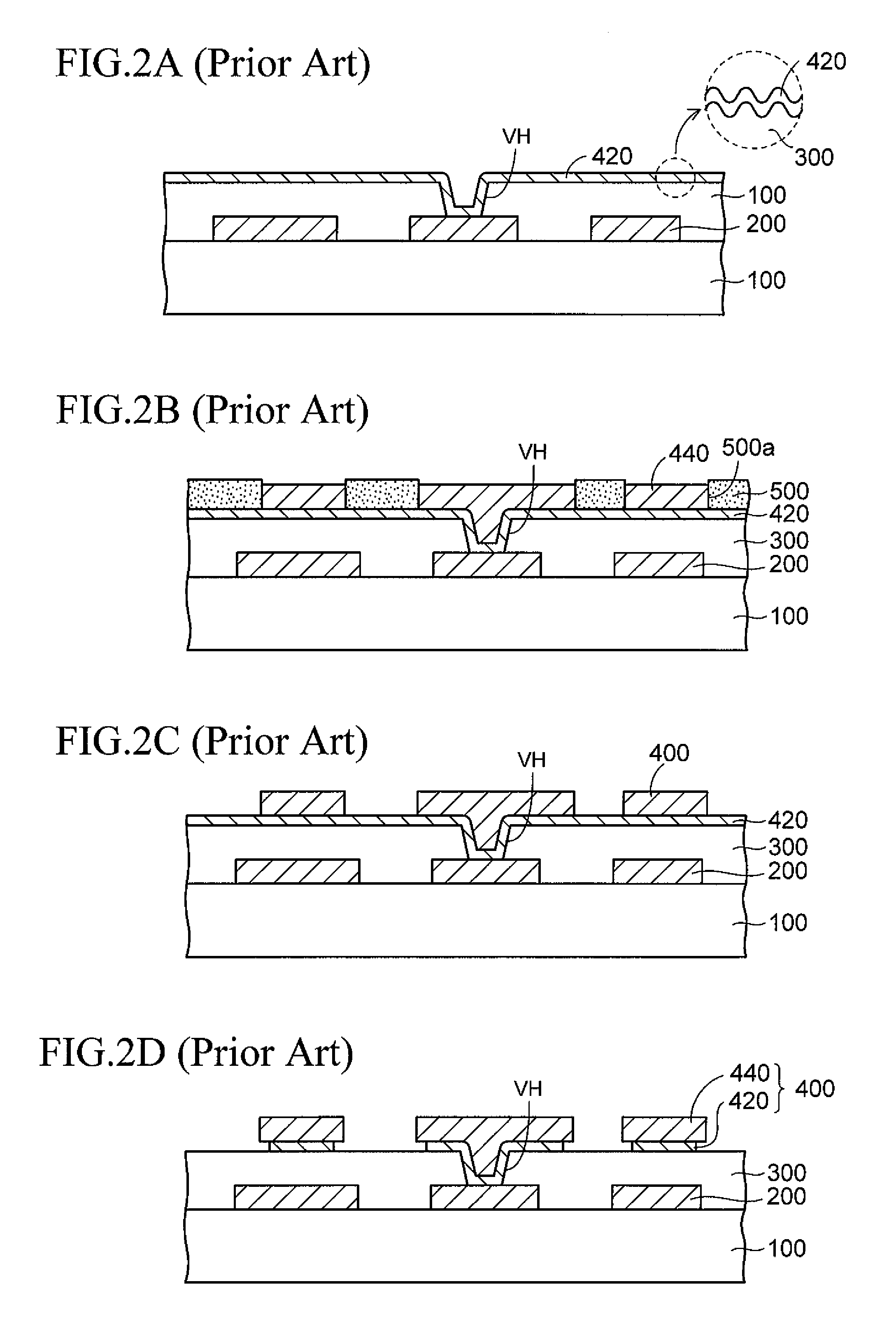
Thus, unevenness of the surface thereof becomes considerably large.
Therefore, a line width becomes considerably thinner than a design specification, and furthermore the pattern jump (pattern disappearance) of the wiring layer is caused.
In this manner, in the prior art, when the line:space of the wiring layer is less than 15:15 μm in a design rule, it is difficult to form the wiring layer according to a design specification with good yield.

Method used


Image

  • Wiring substrate and method of manufacturing the same
  • Wiring substrate and method of manufacturing the same
  • Wiring substrate and method of manufacturing the same

Examples


first embodiment

[0042]FIGS. 4A to 4C, FIGS. 5A to 5C, FIGS. 6A to 6C, and FIGS. 7A to 7C are sectional views showing a method of manufacturing a wiring substrate according to a first embodiment of the present invention. In the method of manufacturing the wiring substrate according to the first embodiment, as shown in FIG. 4A, first, a first wiring layer 20 made of copper, or the like and shaped into a pattern is formed on a substrate 10. As the method of forming the first wiring layer 20, various methods such as the semi-additive process described later, and the like can be employed.

[0043]As an underlying layer on which the first wiring layer 20 is formed, the substrate 10 (glass epoxy resin, or the like) is illustrated. In this case, an insulating layer formed on the substrate 10, or the like may be employed. As the substrate 10, either a rigid type or a flexible type may be employed.

[0044]Then, as shown in FIG. 4B, a film with protection layer 32 in which a protection layer 36 is provided on a re...

second embodiment

[0080]FIGS. 8A to 8C, FIGS. 9A to 9C, FIGS. 10A to 10C, and FIGS. 11A and 11B are sectional views showing a method of manufacturing a wiring substrate according to a second embodiment of the present invention, and FIG. 12 is a sectional view showing an example of the wiring substrate according to the same.

[0081]A difference of the second embodiment from the first embodiment resides in that the second roughening step (FIG. 6A) of roughening the surface of the interlayer insulating layer 30 in the first embodiment is omitted. In the second embodiment, detailed explanation of the same steps as those in the first embodiment will be omitted.

[0082]In the method of manufacturing the wiring substrate according to the second embodiment, like the first embodiment, as shown in FIG. 8A, first, the first wiring layer 20 made of copper, or the like and shaped into the pattern is formed on the substrate 10.

[0083]Then, as shown in FIG. 8B, a film with metal layer 33 in which a metal layer 37 (prote...


PUM


Abstract

A method of manufacturing a wiring substrate of the present invention, includes a step of forming a first wiring layer on an underlying layer, a step of forming a stacked body in which a protection layer is provided on an insulating layer, on the first wiring layer, a step of forming a via hole reaching the first wiring layer by processing the protection layer and the insulating layer, a step of roughening a side surface of the via hole by applying a desmear process to an inside of the via hole while using the protection layer as a mask, a step of removing the protection layer, and a step of forming a second wiring layer, which is connected to the first wiring layer via the via hole, on the insulating layer. The second wiring layer may be formed after the surface of the insulating layer is roughened, or the second wiring layer may be formed without roughening of the surface of the insulating layer.

Description

CROSS-REFERENCE TO RELATED APPLICATIONS[0001]This application is based on and claims priority of Japanese Patent Application No. 2008-137979 filed on May 25, 2008 and Japanese Patent Application No. 2008-199728 filed on Aug. 1, 2008, the entire contents of which are incorporated herein by reference.BACKGROUND OF THE INVENTION[0002]1. Field of the Invention[0003]The present invention relates to a wiring substrate and a method of manufacturing the same and, more particularly, a wiring substrate and a method of manufacturing the same, which is applicable to a substrate of a semiconductor package.[0004]2. Description of the Related Art[0005]In the prior art, there is the build-up wiring board having the multilayer wiring in which a wiring layer and a resin layer are formed alternately on a substrate. In the method of manufacturing the build-up wiring board in the prior art, as shown in FIG. 1A, first, a first wiring layer 200 is formed on a substrate 100. Then, as shown in FIG. 1B, an i...

Claims


Application Information

Patent Timeline
IPC IPC(8): H05K1/11H01B13/00C25D5/02
CPCH01L21/4846H01L21/486H01L2924/0002H01L23/498H01L23/49827H01L23/49894H05K3/0035H05K3/0055H05K3/381H05K3/4644H05K3/4661H05K2203/095H05K2203/1152H05K2203/1383H05K2203/1388H01L2924/00
Inventor KONDO, HITOSHISHIMODAIRA, TOMOYUKIKODAIRA, TADASHI
Owner SHINKO ELECTRIC IND CO LTD
Learn More