Semiconductor device and a method for manufacturing the semiconductor device

a semiconductor device and semiconductor technology, applied in semiconductor devices, semiconductor/solid-state device details, electrical devices, etc., can solve the problem of difficult to ensure the grounding of semiconductor elements, and achieve the effect of preventing the coupling resistance between the semiconductor chip and the grounding layer of the first substra

Inactive Publication Date: 2009-11-26
RENESAS ELECTRONICS CORP
View PDF3 Cites 17 Cited by
  • Summary
  • Abstract
  • Description
  • Claims
  • Application Information

AI Technical Summary

Benefits of technology

[0014]According to the above-described aspect of the present invention, the heat releasing member is electrically coupled with the semiconductor chip, and the tip of the side surface section is coupled with the grounding layer of the first substrate. Therefore, it is configured that the semiconductor chip is grounded to the first substrate through the heat releasing member. Here, since the heat releasing member has the ceiling section covering the surface of the semiconductor chip and the side surface section, which are formed to compose an integral member, a generation of a larger coupling resistance between the semiconductor chip and the grounding layer of the first substrate can be prevented. This allows ensuring a grounding of the semiconductor chip. Further, the tip of the side surface section of the heat releasing member is inserted in the hole of the first substrate, and is fixed in the inside of the hole by an electroconductive material, and the tip of the side surface section is electrically coupled with the grounding layer through the electroconductive material filling the hole. This allows ensuring the contact between the tip of the side surface section of the heat releasing member and the grounding layer, thereby ensuring the grounding of the semiconductor chip.

Problems solved by technology

There are the following problems in the semiconductor devices having the above-described configurations.
Therefore, it becomes difficult to ensure the semiconductor element to be grounded.

Method used


Image

  • Semiconductor device and a method for manufacturing the semiconductor device
  • Semiconductor device and a method for manufacturing the semiconductor device
  • Semiconductor device and a method for manufacturing the semiconductor device

Examples


first embodiment

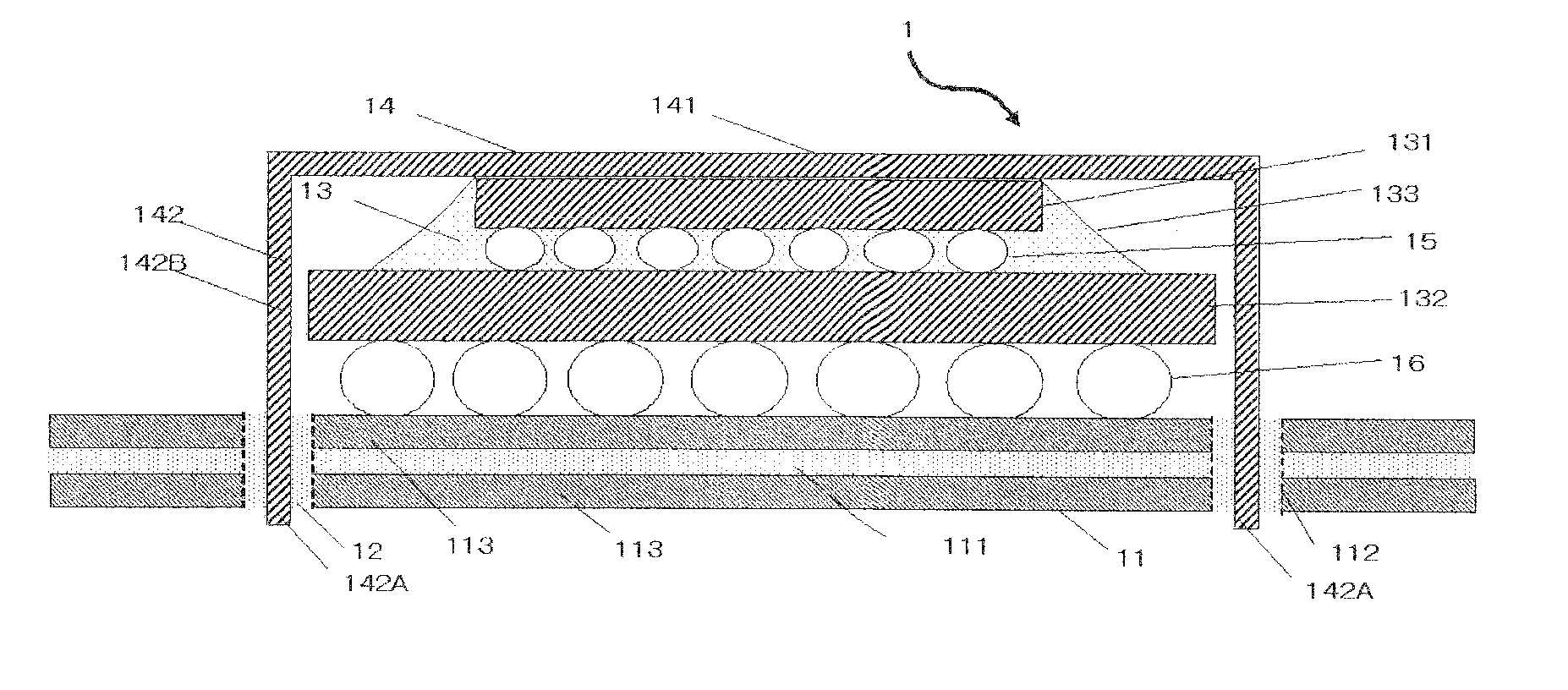
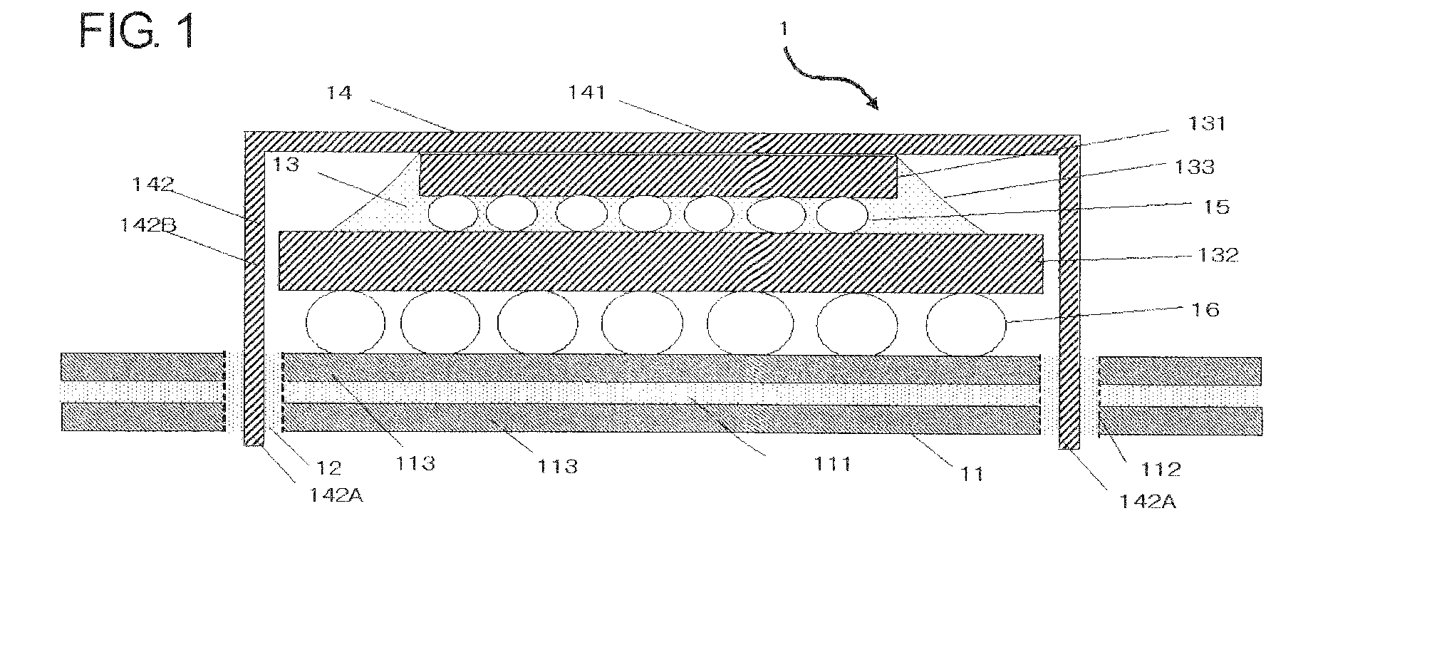
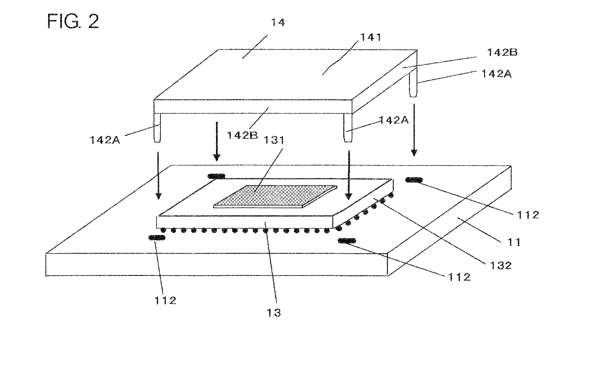
[0029]In the beginning, a semiconductor device 1 of the present embodiment will be described, in reference to FIG. 1. The semiconductor device 1 of the present embodiment includes: a first substrate 11, having a grounding layer 111, and also having holes 112 formed therein for being filled with an electroconductive material 12; a semiconductor chip 131 disposed over such first substrate; and an electroconductive heat releasing member 14, electrically coupled to the semiconductor chip 131 and capable of releasing heat from the semiconductor chip 131. The heat releasing member 14 includes a ceiling section 141 covering the surface of the semiconductor chip 131 and side surface sections 142 extending from the ceiling section 141 toward the sides of the first substrate 11. The ceiling section 141 of the heat releasing member 14 and the side surface sections 142 are formed to compose an integral member. Tips 142A of the side surface sections 142 are inserted in the respective holes 112 o...

second embodiment

[0048]Second embodiment of the present invention will be described in reference to FIG. 6. In the present embodiment, the first substrate 21 has a grounding interconnect 210 in a surface thereof opposite to the surface in the side having the semiconductor chip 131. The grounding interconnect 210 is coupled to a feeding connector (not shown), which is provided for providing a grounding electric potential for the grounding interconnect 210. Other configurations of the first substrate 21 are similar to the first substrate 11. The tips 142A of the heat releasing member 14 are protruded from the apertures of the holes 112, and the tip 142A of the side surface section 142 is coupled to the grounding interconnect 210 through the electroconductive material 12 supplied in the holes 112. Other configurations are similar to the previous embodiment.

[0049]According to the present embodiment described above, the following advantageous effects can be obtained, in addition to enjoying the same adva...


PUM


Abstract

A semiconductor device includes: a first substrate, having a grounding layer and holes formed therein for filling with an electroconductive material; a semiconductor chip over such first substrate; and an electroconductive heat releasing member, electrically coupled to the semiconductor chip able to release heat from the semiconductor chip. The heat releasing member includes a ceiling section covering the surface of the semiconductor chip and side surface extending from the ceiling section toward the sides of the first substrate. The ceiling section of the heat releasing member and the side surface sections are formed to compose an integral member. Tips of the side surface sections are inserted in the respective holes of the first substrate. The tips of the side surface section, in turn, are fixed in the inside of the respective holes with the electroconductive material, and the tips are electrically coupled to the grounding layer through the electroconductive material.

Description

[0001]This application is based on Japanese patent application No. 2008-136,575, the content of which is incorporated hereinto by reference.BACKGROUND[0002]1. Technical Field[0003]The present invention relates to a semiconductor device and a method for manufacturing a semiconductor device.[0004]2. Related Art[0005]Conventionally, a manner for installing a circuit board having a semiconductor chip installed on a motherboard of a printed board and the like is adopted. For example, a circuit board is mounted on a printed circuit board through a ball grid array or the like, and a semiconductor chip is installed on such circuit board through the ball grid array. In such semiconductor device, a surface (semiconductor substrate) of the semiconductor chip in the side opposite to the circuit board is required to be grounded to the printed board.[0006]For example, Japanese Patent Laid-Open No. 2003-100,924 discloses a semiconductor device 700 shown in FIG. 7. The semiconductor device 700 incl...

Claims


Application Information

Patent Timeline
Patent Type & Authority Applications(United States)
IPC IPC(8): H01L23/34H01L21/50
CPCH01L23/3128H01L23/3675H01L2924/15311H01L2224/73253H01L2224/73204H01L2224/32245H01L2224/32225H01L2224/16225H01L23/4093H01L2924/00
Inventor HORIE, MASANAO
Owner RENESAS ELECTRONICS CORP
Why Eureka
Try Eureka