

Photoalignment material, display substrate having an alignment layer formed using the same, and to a method of manufacturing the display substrate
a technology of alignment layer and photoalignment material, which is applied in the direction of instruments, coatings, transportation and packaging, etc., can solve the problems of reducing the method of photoisomerization, affecting the appearance of the display substrate, so as to improve the image quality, reliability and productivity of the display device, and reduce the cost of developing a novel alignment polymer
- Summary
- Abstract
- Description
- Claims
- Application Information
AI Technical Summary
Benefits of technology
Problems solved by technology
Method used
Image

Examples
example 1
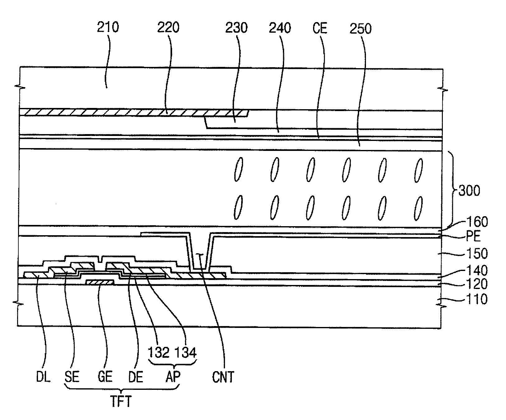
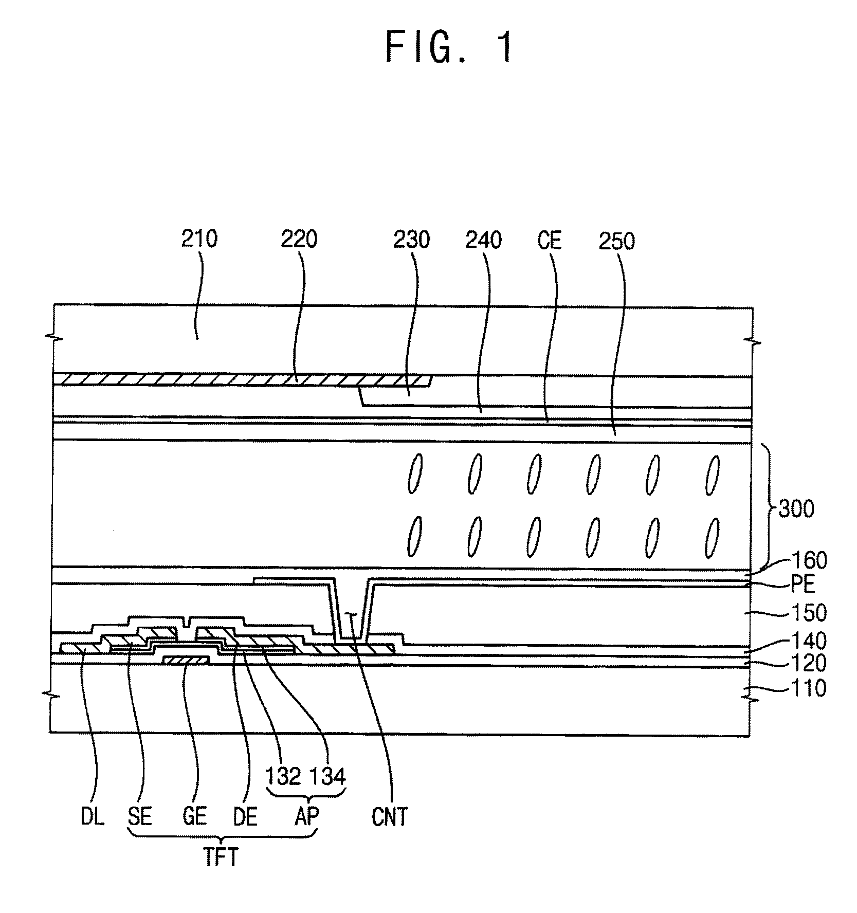
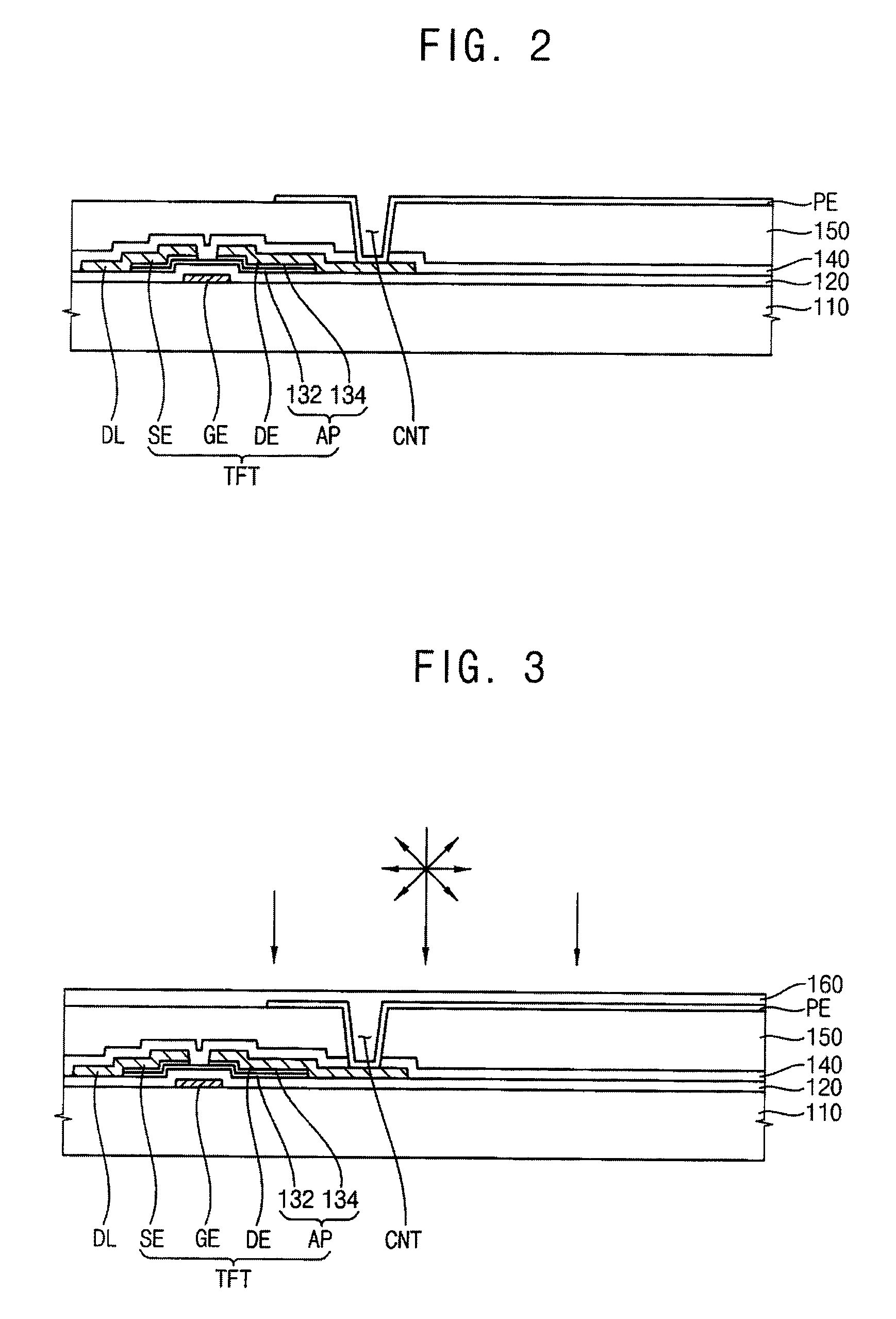
[0059]About 10% by weight of Kapton-H (trade name, manufactured by Dupont, U.S.A.), prepared by reacting 4,4′-diamino-diphenylether with pyromellitic dianhydride in chlorobenzene and containing a repeating unit represented by the following Chemical Formula 6, about 3% by weight of a compound represented by the following Chemical Formula 2 as a photoalignment additive and about 87% by weight of an organic solvent were mixed with each other to prepare a photoalignment material. The organic solvent included about 40% by weight of γ-butyrolactone, about 30% by weight of N-methyl pyrrolidone and about 30% by weight of butyl cellosolve based on the total weight of the organic solvent.
[0060]Evaluation of an Alignment Layer
[0061]The photoalignment material of Example 1 was coated on a 17-inch display substrate, and then prebaked at about 60° C., and then cured at about 200° C. for about 10 minutes. Thereafter, ultraviolet (UV) light of about 1 J / cm2 was irradiated onto the substrate in an a...
PUM
| Property | Measurement | Unit |
|---|---|---|
| temperature | aaaaa | aaaaa |
| pretilt angle | aaaaa | aaaaa |
| temperature | aaaaa | aaaaa |
Abstract
Description
Claims
Application Information