Dual function data register

a data register and dual function technology, applied in the field of nonvolatile memories, can solve the problems of otp memory programming speed being relatively slow, otp memory may not have sufficient current to program all the selected memory cells, and the leakage of salicided transistors, so as to achieve the effect of mitigate at least one disadvantage of prior otp memories

Active Publication Date: 2009-11-26
SYNOPSYS INC
View PDF23 Cites 206 Cited by
  • Summary
  • Abstract
  • Description
  • Claims
  • Application Information

AI Technical Summary

Benefits of technology

[0023]It is an object of the present invention to obviate or mitigate at least one disadvantage of prior OTP memories. More specifically, it is an object of the present invention provide a data register that can integrate program verify operations with data storage functionality.

Problems solved by technology

It is well known that salicided transistors are known to have higher leakage and therefore lower breakdown voltage.
The programming speed of OTP memories is relatively slow, since each programming cycle will attempt to program a certain number of data words at the same time.
Because a large number of bits may be programmed simultaneously, the finite on-chip high voltage generators may not have sufficient current to program all the selected memory cells.
This is especially problematic for anti-fuse transistors.
One of the main problems with this program verify scheme is that the circuit implementation consumes too much valuable circuit area.
The logic required to disable successfully programmed bit positions can be complex, as can be the comparison logic used to detect the failed programming of at least one bit position.
Those skilled in the art will understand that increased circuit area will directly impact the manufacturing cost of the device as more chip area is required per device.

Method used


Image

  • Dual function data register
  • Dual function data register
  • Dual function data register

Examples


Embodiment Construction

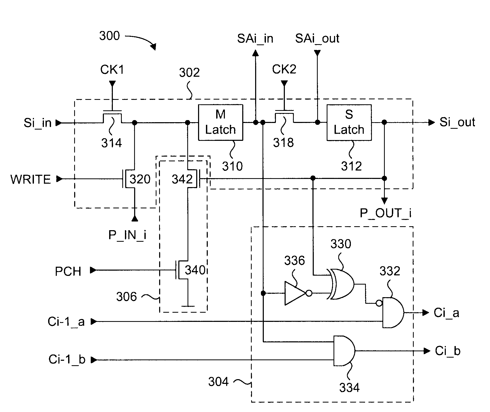
[0063]Generally, the present invention is directed to a dual function serial and parallel data register with integrated program verify functionality. The dual function serial and parallel operation gives the user the option for serial or parallel data interfacing in a single circuit, while integrating program verify functionality for reducing circuit logic overhead by utilizing the master and slave latching circuits of the data register to concurrently store two different words of data. In a program verify operation, the master latch stores program data and the slave latch will receive and store read data. Comparison logic in each register stage will compare the data of both latches and integrate the comparison result to that of the previous register stage. The final single bit result will indicate the presence of at least one bit that has not been programmed. If reprogramming is necessary, automatic program inhibit logic in each stage will prevent successfully programmed bits from ...


PUM


Abstract

A dual function serial and parallel data register with integrated program verify functionality. The master and slave latching circuits of the dual function data register can concurrently store two different words of data. In a program verify operation, the master latch stores program data and the slave latch will receive and store read data. Comparison logic in each register stage will compare the data of both latches, and integrate the comparison result to that of the previous register stage. The final single bit result will indicate the presence of at least one bit that has not been programmed. Automatic program inhibit logic in each stage will prevent successfully programmed bits from being re-programmed in each subsequent reprogram cycle. Either data word can be serially clocked out by selectively starting the shift operations on either the low or high active logic level of a clock signal.

Description

CROSS REFERENCE TO RELATED APPLICATIONS[0001]This application claims the benefit of priority of U.S. Provisional Patent Application No. 60 / 871,519 filed Dec. 22, 2006, and U.S. Provisional Patent Application No. 60 / 871,571 filed Dec. 22, 2006, both of which are incorporated herein by reference in their entirety.FIELD OF THE INVENTION[0002]The invention is directed to non-volatile memories. More specifically, the invention is directed to data registers of non-volatile memories.BACKGROUND OF THE INVENTION[0003]Over the past 30 years, anti-fuse technology has attracted significant attention of many inventors, IC designers and manufacturers. An anti-fuse is a structure alterable to a conductive state, or in other words, an electronic device that changes state from not conducting to conducting. Equivalently, the binary states can be either one of high resistance and low resistance in response to electric stress, such as a programming voltage or current. There have been many attempts to d...

Claims


Application Information

Patent Timeline
Patent Type & Authority Applications(United States)
IPC IPC(8): G11C7/10G11C7/00H03K19/173H03K3/289
CPCG11C16/3454G11C16/3459G11C17/14G11C17/16G11C5/143G11C19/00G11C29/027G11C29/52G11C2029/0407G11C17/165
Inventor KURJANOWICZ, WLODEK
Owner SYNOPSYS INC
Why Eureka
Try Eureka