
Semiconductor contact formation system and method

a technology of semiconductor integrated circuits and contact formation systems, applied in the direction of semiconductor/solid-state device details, electrical apparatus, semiconductor devices, etc., can solve the problems of difficult optimization, complex semiconductor integrated circuit manufacturing efforts, and high requirements for greater functionality, and achieve the effect of facilitating contact formation, small substrate connection, and compact high-density components

Active Publication Date: 2009-12-03
MONTEREY RES LLC
View PDF8 Cites 0 Cited by
  • Summary
  • Abstract
  • Description
  • Claims
  • Application Information

AI Technical Summary

Benefits of technology

"The present invention is a system and method for creating semiconductor contacts. It uses multiple etch stop layers to form insulation regions that facilitate the creation of small connections between substrates and metal layers. This process addresses critical dimension concerns and allows for the creation of reliable, compact high-density components like flash memory cells. The method also involves depositing electrical conducting material in the contact region. Overall, the invention provides a reliable and efficient way to create semiconductor contacts."

Problems solved by technology

Integrated circuits typically include contact regions for conducting electricity (e.g., between active components) and it is often very difficult to achieve optimized results within requisite narrow tolerances when attempting to fabricate precise contact regions that operate properly.
Semiconductor integrated circuit manufacturing efforts are usually complicated by ever increasing demands for greater functionality.
More complicated circuits are usually required to satisfy the demand for greater functionality.
However, including more components within an integrated circuit often requires the components to be densely packed in relatively small areas and reliably packing a lot of components in relatively small areas of an integrated circuit (IC) is usually very difficult.
However, decreases in contact sizes are usually limited by contact void creation processes (such as lithographic etching processes).
Standard lithographic etching and removal processes traditionally have difficulty producing relatively small contact voids.
Complex processes that attempt to create smaller voids are often cost prohibitive or nonfeasible.
While decreasing the size of a contact usually permits greater component densities, there are usually physical limitations on how small the contact can become and still operate properly.
Interconnection phenomenon such as electromigration can cause reliability problems as the dimension of the contact becomes very small.
For example, electromigration can cause discontinuities in conducting materials if the dimensions are too small.
Fabrication of small contacts with desirable CD characteristics can be challenging.
Without proper component insulation there is a tendency for detrimental interactions between component parts to occur that hinder proper and reliable operation.
For example, placement of more components in smaller spaces by reducing the separation between adjacent component parts often increases the probabilities of failures associated with leakage currents.
While introduction of complex and complicated lithographic techniques may attempt to provide small size components, these advance techniques usually consume significant resources and are very expensive.

Method used


Image

  • Semiconductor contact formation system and method
  • Semiconductor contact formation system and method
  • Semiconductor contact formation system and method

Examples


Embodiment Construction

[0021]Reference will now be made in detail to the preferred embodiments of the invention, examples of which are illustrated in the accompanying drawings. While the invention will be described in conjunction with the preferred embodiments, it will be understood that they are not intended to limit the invention to these embodiments. On the contrary, the invention is intended to cover alternatives, modifications and equivalents, which may be included within the spirit and scope of the invention as defined by the appended claims. Furthermore, in the following detailed description of the present invention, numerous specific details are set forth in order to provide a thorough understanding of the present invention. However, it will be obvious to one ordinarily skilled in the art that the present invention may be practiced without these specific details. In other instances, well known methods, procedures, components, and circuits have not been described in detail as not to unnecessarily o...


PUM


Abstract

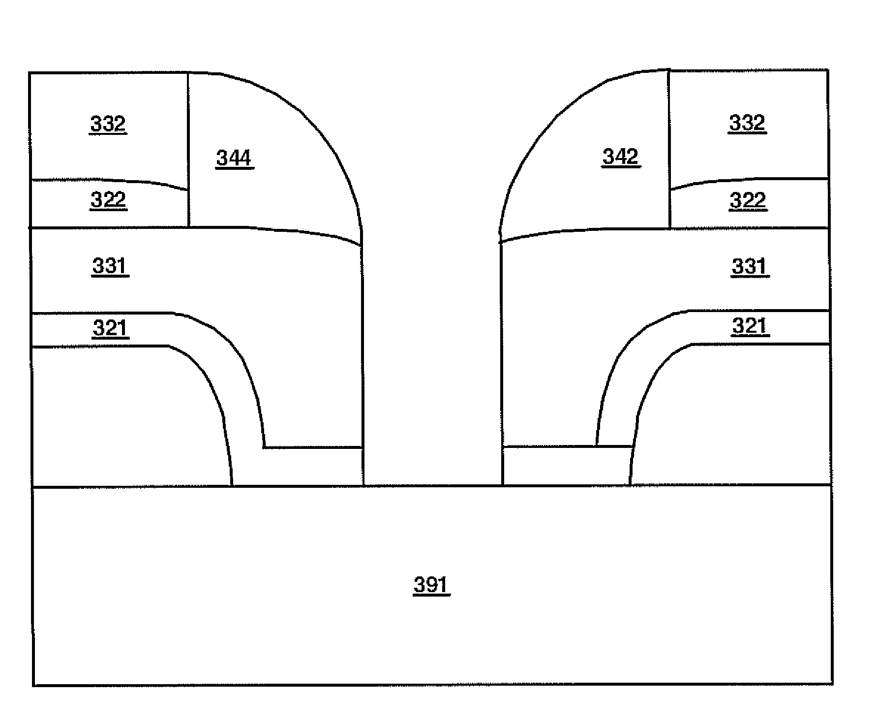
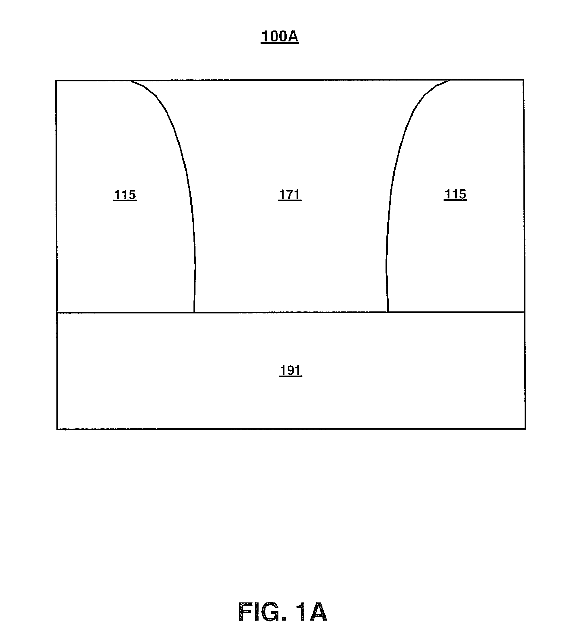
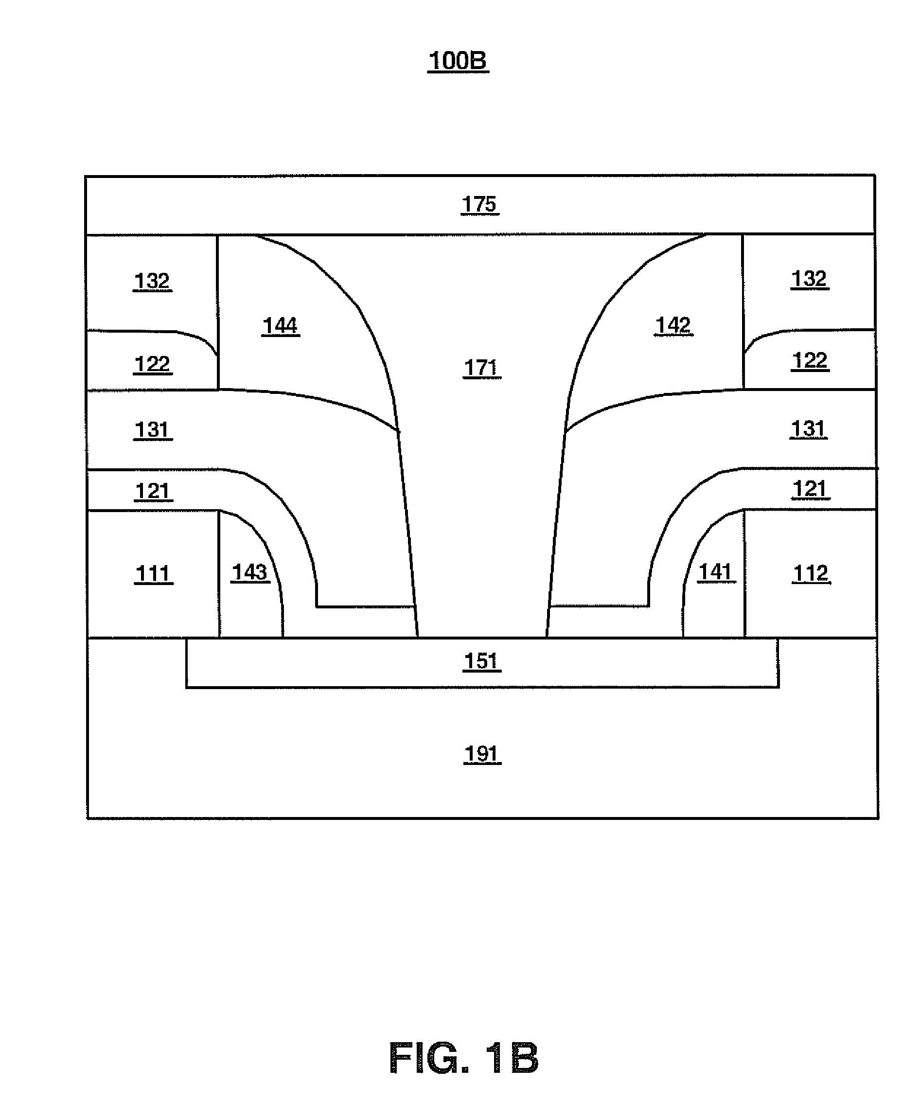
The present invention is a semiconductor contact formation system and method. Contact insulation regions are formed with multiple etch stop sublayers that facilitate formation of contacts. This contact formation process provides relatively small substrate connections while addressing critical lithographic printing limitation concerns in forming contact holes with small dimensions. In one embodiment, a multiple etch stop insulation layer comprising multiple etch stop layers is deposited. A contact region is formed in the multiple etch stop insulation layer by selectively removing (e.g., etching) some of the multiple etch stop insulation layer. In one embodiment, a larger portion of the multiple etch stop insulation layer is removed close to the metal layer and a smaller portion is removed closer to the substrate. The different contact region widths are achieved by performing multiple etching processes controlled by the multiple etch stop layers in the multiple etch stop insulation layer and spacer formation to shrink contact size at a bottom portion. Electrical conducting material (e.g., tungsten) is deposited in the contact region.

Description

RELATED APPLICATIONS[0001]This application is a divisional of and claims the benefit of co-pending application Ser. No. 10 / 934,828 (Attorney docket No. SPSN-H0638) entitled A SEMICONDUCTOR CONTACT FORMATION SYSTEM AND METHOD, filed Sep. 2, 2004, which is incorporated herein by reference.TECHNICAL FIELD[0002]The present claimed invention relates to the field of semiconductor contact fabrication. More particularly, the present invention relates to a semiconductor contact fabrication system and method that utilizes multiple etch stop layers.BACKGROUND ART[0003]Electronic systems and circuits have made a significant contribution towards the advancement of modern society and are utilized in a number of applications to achieve advantageous results. Numerous electronic technologies such as digital computers, calculators, audio devices, video equipment, and telephone systems have facilitated increased productivity and reduced costs in analyzing and communicating data, ideas and trends in mo...

Claims


Application Information

Patent Timeline
Patent Type & Authority Applications(United States)
IPC IPC(8): H01L23/522
CPCH01L21/76804H01L21/76816H01L21/76829H01L21/76831H01L2924/0002H01L23/485H01L2924/00
Inventor LI, WENMEIHUI, ANGELA T.HOPPER, DAWNGHANDEHARI, KOUROS
Owner MONTEREY RES LLC
Learn More