
Wiring substrate and semiconductor package

a technology of wiring substrate and semiconductor package, which is applied in the direction of printed circuit manufacturing, printed circuit aspects, electrical apparatus construction details, etc., can solve problems such as migration progress

Active Publication Date: 2009-12-03
SHINKO ELECTRIC IND CO LTD
View PDF6 Cites 25 Cited by
  • Summary
  • Abstract
  • Description
  • Claims
  • Application Information

AI Technical Summary

Benefits of technology

The present invention relates to a wiring substrate and a semiconductor package. More specifically, it addresses the issue of potential electrical shortcircuiting between adjacent lines of wiring in a semiconductor package caused by the migration of metal ions from the wiring. The invention proposes a solution by eliminating the contact between the filler and the wiring, reducing the grain diameter of the filler, and preventing the ionization of metal. The technical effect of the invention is to improve the reliability and stability of semiconductor packages.

Problems solved by technology

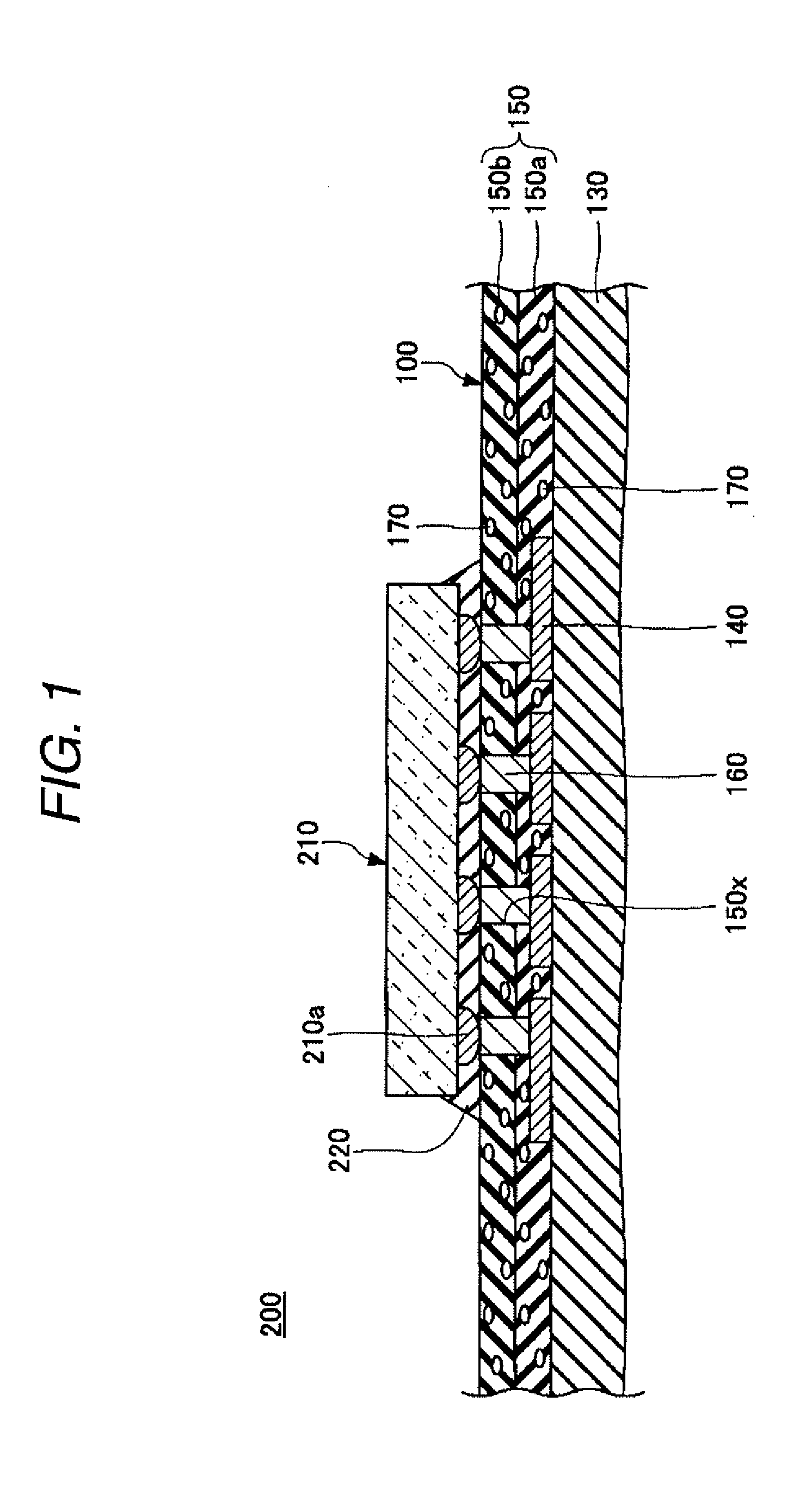
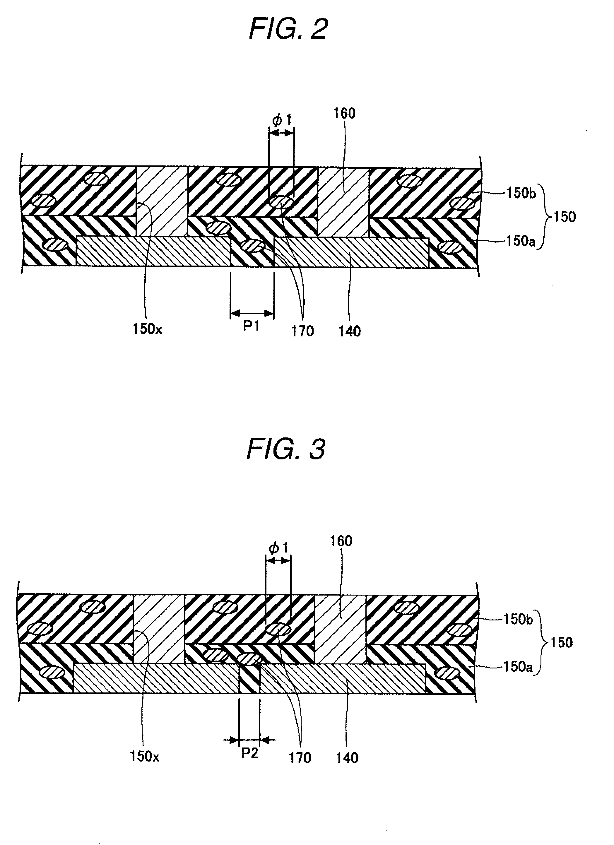
For this reason, there has been a problem in that the migration progresses due to the presence of the filler 170.

Method used


Image

  • Wiring substrate and semiconductor package
  • Wiring substrate and semiconductor package
  • Wiring substrate and semiconductor package

Examples


first embodiment

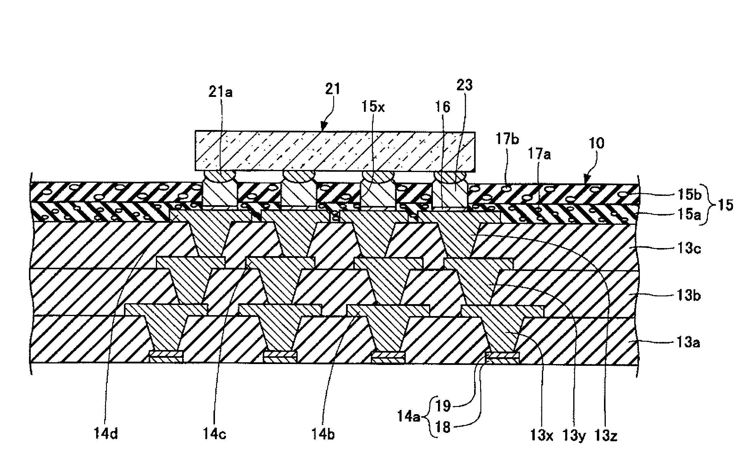
[0091]In a first embodiment, an example is shown in which the invention is applied to a wiring substrate having a multilayered wiring layer (built-up wiring layers). FIG. 4 is a cross-sectional view illustrating a wiring substrate having built-up wiring layers in accordance with the first embodiment of the invention. Referring to FIG. 4, a wiring substrate 10 is a wiring substrate provided with built-up wiring layers including a first insulating layer 13a, a second insulating layer 13b, a third insulating layer 13c, a wiring 14a, a wiring 14b, a wiring 14c, a wiring 14d, a solder resist layer 15, and a metal layer 16.

[0092]In the wiring substrate 10, the wiring 14a is formed in a wiring layer which is a lowermost layer (hereinafter referred to as the “first wiring layer”). The first insulating layer 13a is formed so as to cover the wiring 14a, and the wiring 14b is formed on the first insulating layer 13a. Further, the second insulating layer 13b is formed so as to cover the wiring ...

second embodiment

[0141]In a second embodiment, an example is shown in which the invention is applied to a semiconductor package provided with a wiring substrate having built-up wiring layers. FIG. 21 is a cross-sectional view illustrating a semiconductor package in accordance with the second embodiment of the invention. In FIG. 21, those components that are identical to those shown in FIG. 4 will be denoted by the same reference numerals, and a description will be omitted in some cases. Referring to FIG. 21, a semiconductor package 20 has the wiring substrate 10 shown in FIG. 4, a semiconductor chip 21, and an underfill resin 22. A pre-solder 23 is formed on the metal layer 16 of the wiring substrate 10 by such as the application of solder paste. The metal layer 16 and the pre-solder 23 are electrically connected.

[0142]The semiconductor chip 21 is one in which a semiconductor integrated circuit (not shown) and electrode pads (not shown) are formed on a semiconductor substrate (not shown) formed of s...

third embodiment

[0149]In a third embodiment, an example is shown in which the invention is applied to a semiconductor package (so-called chip size package: CSP) of a chip size which is substantially identical to that of a semiconductor chip in a plan view. FIG. 23 is a cross-sectional view illustrating a semiconductor package in accordance with the third embodiment of the invention. Referring to FIG. 23, a semiconductor package 30 has a semiconductor chip 31, internal connection terminals 32, an insulating layer 33, a wiring 34, a solder resist layer 36, and external connection terminals 37.

[0150]FIG. 24 is a plan view of a semiconductor substrate for forming the semiconductor package in accordance with the third embodiment of the invention. In FIG. 24, reference numeral 51 denotes a semiconductor wafer, and reference character C denotes a position (hereafter referred to as the “wafer cutting position C”) at which a dicer cuts the semiconductor wafer 51. The semiconductor wafer 51 is provided with ...


PUM

PropertyMeasurementUnit
grain diameter φ1aaaaaaaaaa
grain diameter φ2aaaaaaaaaa

Abstract

A wiring substrate includes: an insulating layer; a wiring formed on the insulating layer; and a solder resist layer formed on the insulating layer so as to cover at least a portion of the wiring, the solder resist layer being constituted by a plurality of layers, wherein the plurality of layers contain fillers of different grain diameters, a layer thickness of an innermost layer for constituting the plurality of layers is thicker than a layer thickness of the wiring, and a grain diameter of the filler contained in the innermost layer is smaller than a shortest interval between adjacent lines of the wiring.

Description

BACKGROUND OF THE INVENTION[0001]The present invention relates to a wiring substrate and a semiconductor package, and more particularly to a wiring substrate having a solder resist layer constituted by a plurality of layers, as well as a semiconductor package having the same.[0002]For example, in a semiconductor package in which a semiconductor chip is mounted on a wiring substrate having built-up wirings, a solder resist layer is formed as an outermost layer of the wiring substrate. A photo solder resist which is photosensitive is generally used as the solder resist layer. In addition, the solder resist layer is generally formed as a two-layered structure for forming a layer of a sufficient thickness.[0003]FIG. 1 is a cross-sectional view partially illustrating a conventional semiconductor package. A semiconductor package 200 has a wiring substrate 100, a semiconductor chip 210, and an underfill resin 220. The wiring substrate 100 has an insulating layer 130, a wiring 140, a solder...

Claims


Application Information

Patent Timeline
Patent Type & Authority Applications(United States)
IPC IPC(8): H05K7/02H05K1/00
CPCH01L21/563H01L2224/16235H01L23/3114H01L23/3171H01L23/49816H01L23/49822H01L23/49827H01L23/49894H01L24/13H01L24/16H01L2221/68345H01L2224/0231H01L2224/13022H01L2224/13099H01L2224/16H01L2224/73203H01L2924/01013H01L2924/0102H01L2924/01022H01L2924/01029H01L2924/01046H01L2924/01075H01L2924/01078H01L2924/01079H01L2924/01082H01L2924/14H01L2924/15174H05K1/0254H05K3/285H05K3/3436H05K3/3452H05K2201/0195H05K2201/0209H05K2201/0266H05K2201/0769H05K2201/10674H01L2924/01005H01L2924/01006H01L2924/01033H01L2924/01045H01L2924/01047H01L23/3192H01L2224/02333H01L2224/0401H01L21/6835H01L2924/12044H01L2924/00
Inventor YAMAMOTO, TAKAYUKI
Owner SHINKO ELECTRIC IND CO LTD
Learn More