
Image Processing Apparatus

a technology for processing apparatus and images, applied in the direction of electrical apparatus, instruments, computing, etc., can solve the problems of large power consumption, more expensive final products, and difficulty in designing electric circuits, so as to reduce the number of accesses to memory, reduce power consumption, and reduce bandwidth

Inactive Publication Date: 2009-12-03
HITACHI CONSUMER ELECTRONICS CORP
View PDF8 Cites 18 Cited by
  • Summary
  • Abstract
  • Description
  • Claims
  • Application Information

AI Technical Summary

Benefits of technology

[0016]According to an aspect of the invention, the image processing apparatus is capable of reducing the number of accesses to memory even when processing image data composed of a massive amount of information and making an effective use of a bandwidth, thereby being able to reduce the power consumption.
[0017]Further, the image processing apparatus is capable of reducing a bandwidth and accessing a memory randomly, so that the apparatus may include more image processing functions. Hence, the resulting image processing apparatus enhances its usability.

Problems solved by technology

The Abstract of this Official Gazette describes “[Solving Problem] Though it is required to enhance a databand width in accessing a memory, a technique for speeding up an outside interface and a memory bus of a memory LSI confronts difficulty on design of electric circuitry.
This frequent access may lead to making the power consumption larger and the final products more costly.
In the LSI to be used for processing the image data, however, a single access is not always given to a memory.
Hence, if the just aforementioned process is executed with respect to one systematic access to memory, the effect of reducing the number of accesses to memory is quite small, so that the reducing effect is restricted.

Method used


Image

  • Image Processing Apparatus
  • Image Processing Apparatus
  • Image Processing Apparatus

Examples


first embodiment

[0035]The description will be oriented to the configuration and the operation of the image processing apparatus according to a preferred embodiment of the present invention.

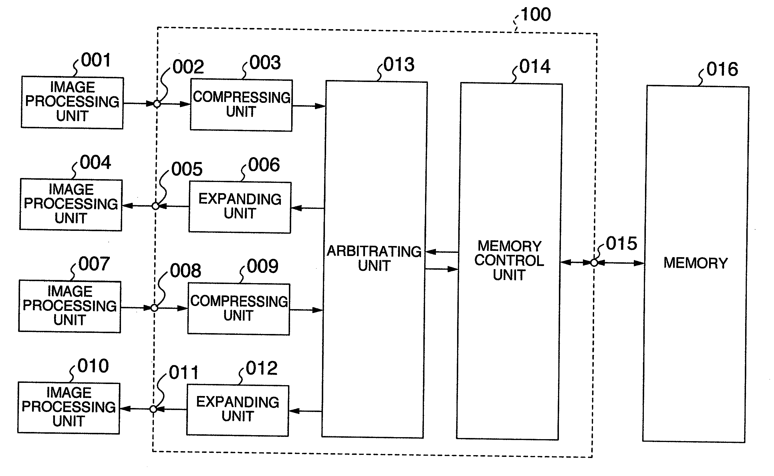
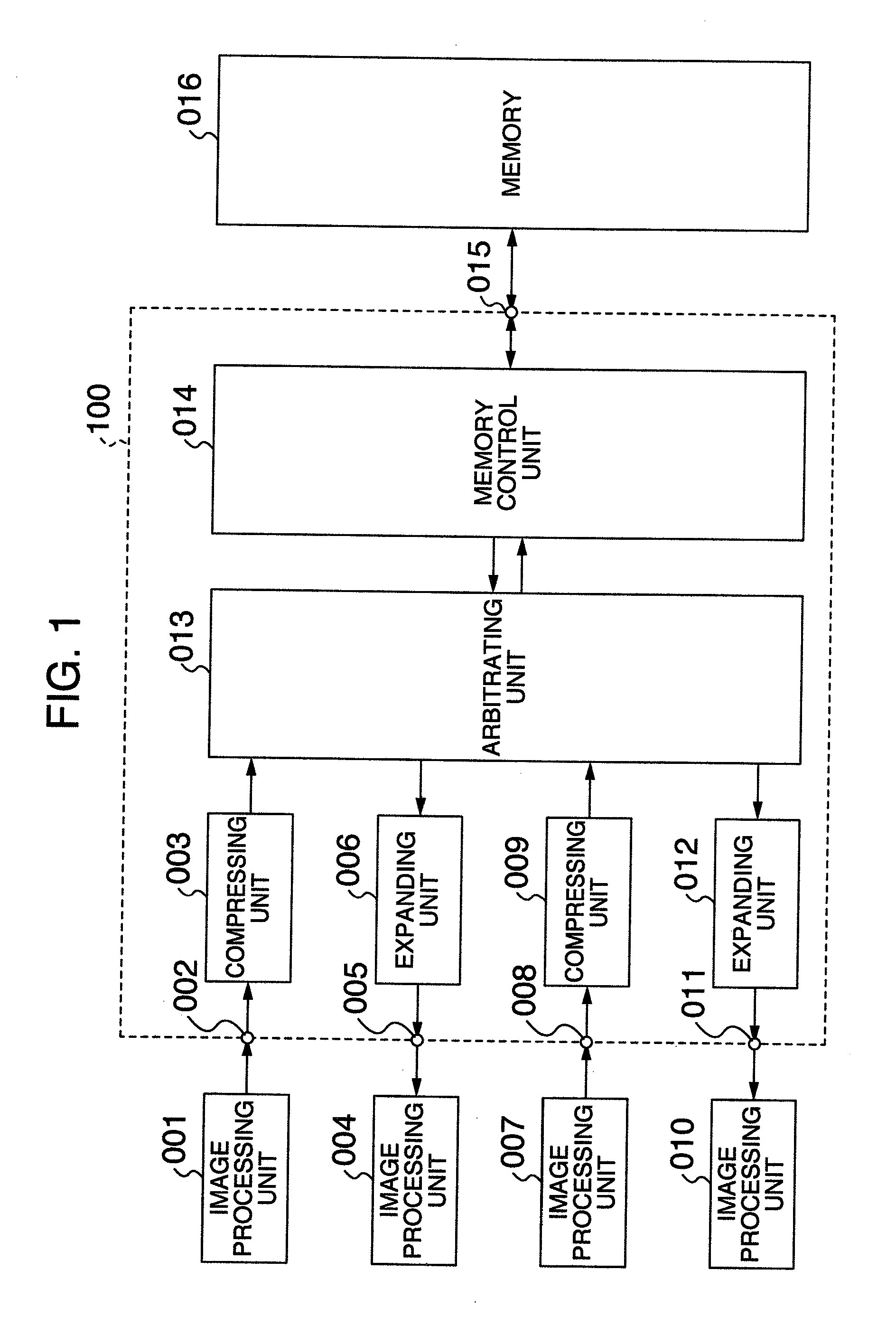
[0036]The configuration of this embodiment will be described with reference to FIG. 1.

[0037]In FIG. 1, the image processing units 001, 004, 007, 010 have a function of processing baseband signals such as a luminance signal and a color difference signal, each of those signals quantized at 8 bits as image data, at a frame unit. For this processing, those processing units need to write or read the data to or from a SDRAM. The baseband signals are inputted into compressing units 003 and 009 through input units 002 and 008 respectively.

[0038]Further, the baseband signals expanded by expanding units 006 and 012 are supplied to the image processing units 004 and 010 through output units 005 and 011 respectively. The compressing units 003, 009 or the expanding units 006, 009 are configured to write or read the image data...

second embodiment

[0067]FIG. 11 shows another embodiment in which the concrete configuration of the image processing unit is embodied. If the shown components includes the components being functionally equal to those described with respect to the foregoing embodiments, these components are denoted by the same reference numbers as those of the foregoing embodiments, and thus the description thereabout is left out.

[0068]A first image processing unit 020 is served as a noise removing circuit, for example. This unit 020 operates to write the inputted image data in the memory 016 and remove the noise components based on the correlation between the frames.

[0069]Then, an encoder 024 is located as a second image processing unit in the system. The encoder is served to write the image data from which noise components are removed in the memory 016, read the image data from the memory 016 in sequence, and encode the image data so as to generate the coded data.

[0070]A decoder 026 is located as a third image proce...

third embodiment

[0075]FIG. 12 shows the embodiment of the image processing apparatus which is applied to an external bus such as a PCI bus in place of the outside memory such as a DRAM. As mentioned above with respect to the second embodiment, the shown components being functionally equal to those of the foregoing embodiments are denoted by the same reference numbers and are not described below.

[0076]In place of the memory control unit connected between the arbitrating unit 013 and the memory 016, the outside bus control unit 030 is located so that the control unit 030 is connected with an outside bus 032 through the connection unit 031. This location is effective in reducing the number of accesses in not only the memory such as a DRAM but also the PCI bus.

[0077]Hence, the margin occurring in data communications with the outside image processing unit 033 connected with the outside bus 032 makes it possible to communicate a larger amount of information with the outside image processing unit 033.


PUM


Abstract

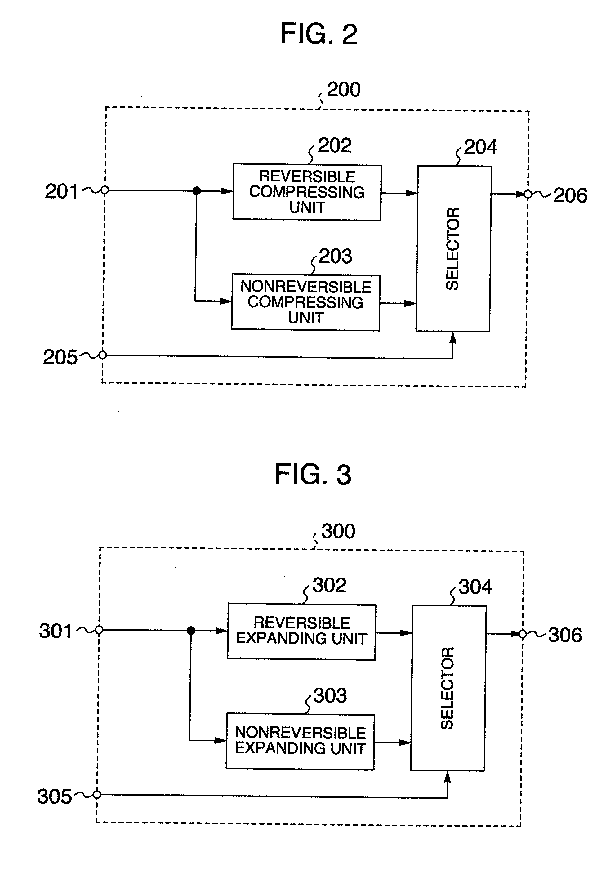
An image processing apparatus is configured to have units for compressing and expanding image data and an arbitrating unit for arbitrating control units for executing image processing so that the compressing and expanding units are located between the arbitrating unit and the control units respectively. The apparatus further includes the circuits for compressing and expanding the image data in a reversible manner and a nonreversible manner so that the compressing and expanding manner may be switched according to the image processing condition. When treating a large amount of image data, this configuration makes it possible to reduce the number of accesses to memory and make effective use of a bandwidth, thereby being able to reduce the power consumption. Since the bandwidth is reduced and the random access to memory is made possible, more image processing capabilities may be provided so that the operability of this apparatus is enhanced.

Description

INCORPORATION BY REFERENCE[0001]The present application claims priority from Japanese application JP2008-138855 filed on May 28, 2008, the content of which is hereby incorporated by reference into this application.BACKGROUND OF THE INVENTION[0002]The present invention relates to an image processing apparatus. More particularly, the invention relates to an image processing system which is required to perform an operation of accessing a moving image or a still image in a memory, representatively, a dynamic random access memory (DRAM).[0003]One of the background arts in the technical field to which the present invention belongs is disclosed in the Official Gazette of JP-A-10-301841. The Abstract of this Official Gazette describes “[Solving Problem] Though it is required to enhance a databand width in accessing a memory, a technique for speeding up an outside interface and a memory bus of a memory LSI confronts difficulty on design of electric circuitry. To overcome this difficulty, it ...

Claims


Application Information

Patent Timeline
Patent Type & Authority Applications(United States)
IPC IPC(8): G06K9/36H04N1/46H04N1/413H04N19/00H04N19/103H04N19/134H04N19/196H04N19/423H04N19/467H04N19/50H04N19/60H04N19/61H04N19/65H04N19/70H04N19/89H04N19/90H04N19/91
CPCH04N19/426
Inventor NONAKA, TOMOYUKIKOMI, HIRONORIINATA, KEISUKEYATABE, YUSUKEOKADA, MITSUHIRO
Owner HITACHI CONSUMER ELECTRONICS CORP
Learn More