Low Power Circuit Structure with Metal Gate and High-k Dielectric

a low-power circuit and dielectric technology, applied in the direction of basic electric elements, electrical apparatus, semiconductor devices, etc., can solve the problems of affecting the achievement of the desired threshold voltage value, affecting the performance improvement of devices of deeply submicron generation, and increasing complexity of technology

Inactive Publication Date: 2009-12-03
GLOBALFOUNDRIES INC
View PDF9 Cites 35 Cited by
  • Summary
  • Abstract
  • Description
  • Claims
  • Application Information

AI Technical Summary

Benefits of technology

[0010]Embodiments of the present invention further disclose a method for producing a circuit structure. The method includes: in the fabrication of an NFET, implementing an NFET gate stack, an NFET gate insulator, and an n-channel, where the n-channel is hosted in a Si based material and underlies the NFET gate insulator, where the NFET gate insulator includes a layer of a first high-k material. The method further includes: implementing a PFET gate stack, a PFET gate insulator, and a p-channel, where the p-channel is hosted in the Si based material and underlies the PFET gate insulator, where the PFET gate insulator includes a layer of a second high-k material. One overlays the first high-k material and the second high-k material with a layer of a cap material, where the first and second high-k materials are in direct physical contact with the layer of the cap material, and overlays the cap material with a layer of a gate metal, where the layer of the cap material and the layer of the gate metal are in direct physical contact. During implementation of the NFET gate stack and the PFET gate stack, producing a portion in the NFET gate stack and in the PFET gate stack by patterning the layers of the cap material and of the gate metal. This portion is identical in the NFET device and in the PFET device. The method also teaches the overlaying the NFET gate stack and a vicinity of the NFET gate stack with a first dielectric layer, and exposing the NFET device and the PFET device to oxygen. The oxygen reaches the second high-k material, and causes a predetermined shift in the threshold voltage of the PFET device, while due to the first dielectric layer oxygen is prevented from reaching the first high-k material and the NFET device threshold remains unchanged.

Problems solved by technology

As FET (Field-Effect-Transistor) devices are being scaled down, the technology becomes more complex, and changes in device structures and new fabrication methods are needed to maintain the expected performance enhancement from one generation of devices to the next.
There is a great difficulty in maintaining performance improvements in devices of deeply submicron generations.
Sometimes such influences are detrimental for achieving the desired threshold voltage values.
Unfortunately, shifting the threshold of both PFET and NFET devices simultaneously, may not easily lead to threshold values in an acceptably tight range for CMOS circuits.
Typically, small FET devices with high-k dielectrics and metal gates require expensive complicated processing.

Method used


Image

  • Low Power Circuit Structure with Metal Gate and High-k Dielectric
  • Low Power Circuit Structure with Metal Gate and High-k Dielectric
  • Low Power Circuit Structure with Metal Gate and High-k Dielectric

Examples


Embodiment Construction

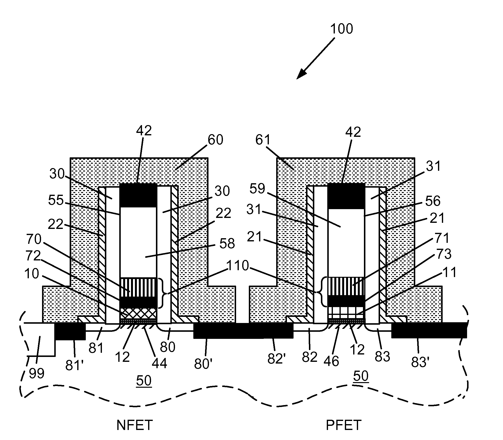
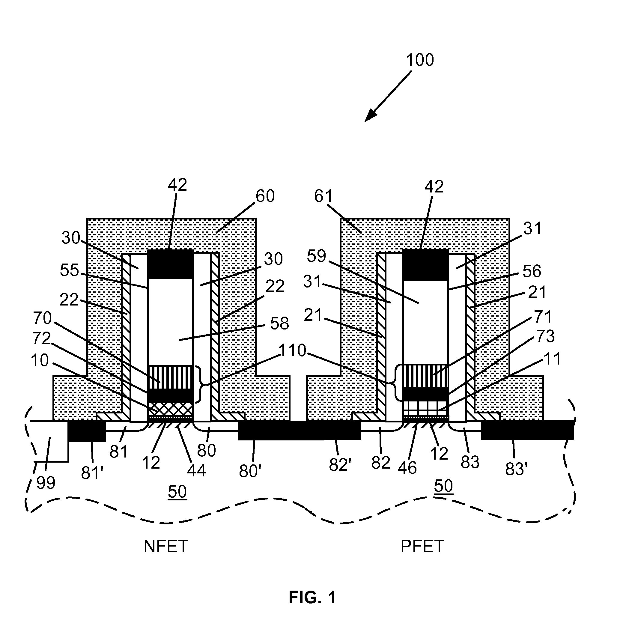
[0019]It is understood that Field Effect Transistor-s (FET) are well known in the electronic arts. Standard components of a FET are the source, the drain, the body in-between the source and the drain, and the gate. The body is usually part of a substrate, and it is often called substrate. The gate is overlaying the body and is capable to induce a conducting channel in the body between the source and the drain. In the usual nomenclature, the channel is hosted by the body. The gate is separated from the body by the gate insulator. There are two type of FET devices: a hole conduction type, called PFET, and an electron conduction type, called NFET. Often, but not exclusively, PFET and NFET devices are wired into CMOS circuits. A CMOS circuit contains at least one PFET and at least one NFET device. In manufacturing, or processing, when NFET and PFET devices are fabricated together on the same chip, one is dealing with CMOS processing and the fabrication of CMOS structures.

[0020]In FET op...


PUM


Abstract

FET device structures are disclosed with the PFET and NFET devices having high-k dielectric gate insulators, metal containing gates, and threshold adjusting cap layers. The NFET gate stack and the PFET gate stack each has a portion which is identical in the NFET device and in the PFET device. This identical portion contains at least a gate metal layer and a cap layer. Due to the identical portion, device fabrication is simplified, requiring a reduced number of masks. Furthermore, as a consequence of using a single layer of metal for the gates of both type of devices, the terminal electrodes of NFETs and PFETs can be butted with each other in direct physical contact. Device thresholds are further adjusted by oxygen exposure of the high-k dielectric. Threshold values are aimed for low power consumption device operation.

Description

CROSS REFERENCE TO A RELATED APPLICATION[0001]This application is a Division of application Ser. No. 11 / 835,318, filed Aug. 7. 2007, which is incorporated herein by reference in its entirety.FIELD OF THE INVENTION[0002]The present invention relates to power conserving electronic circuits. In particular, it relates to circuit structures having high-k containing gate dielectrics and metal containing gates. The invention also relates to ways of adjusting the threshold voltages for suiting low power operation.BACKGROUND OF THE INVENTION[0003]Today's integrated circuits include a vast number of devices. Smaller devices and shrinking ground rules are the key to enhance performance and to reduce cost. As FET (Field-Effect-Transistor) devices are being scaled down, the technology becomes more complex, and changes in device structures and new fabrication methods are needed to maintain the expected performance enhancement from one generation of devices to the next. The mainstay material of mi...

Claims


Application Information

Patent Timeline
Patent Type & Authority Applications(United States)
IPC IPC(8): H01L21/8238
CPCH01L21/823807H01L21/823842H01L29/49H01L29/513H01L29/785H01L29/665H01L29/6656H01L29/7833H01L29/7843H01L29/517
Inventor DORIS, BRUCE B.CARTIER, EDUARD ALBERTLINDER, BARRY PAULNARAYANAN, VIJAYPARUNCHRI, VAMSI
Owner GLOBALFOUNDRIES INC
Why Eureka
Try Eureka