
Circuit and method for compensating display defect in video display

Active Publication Date: 2009-12-10
LG DISPLAY CO LTD
View PDF2 Cites 4 Cited by
  • Summary
  • Abstract
  • Description
  • Claims
  • Application Information

AI Technical Summary

Benefits of technology

[0012]An advantage of the present invention is to provide circuit and method for compensating a display defect in a video display device which can reduce a size of a memory which stores a compensation data on a plurality of regular patterned defective regions.

Problems solved by technology

Though the display panel having the display defect passes through a repair process for the defective portion, there can be display defect that can not be repaired even in the repair process.
The display defect is caused mostly by variation of exposure quantity come from superimposition of the exposures and aberration of multi-lens at the time of multi-exposure by an exposing apparatus used in a thin film pattern forming process.
The variation causes brightness variation on a displayed video, resulting in the display defect.
The display defect in a form of the transverse lines or longitudinal lines can not be solved even with modification of a process technology.
Moreover, the display defect can be displayed as a point defect from a defective pixel having foreign matters infiltrated therein.
Though the defective pixel is repaired in the repair process, the point defect takes place even from the repaired pixel.
If the repair process is performed, in which the pixel turned into a dark point is linked to an adjacent regular pixel, requiring that a data supplied to the regular pixel is spread and charged even to the repaired pixel linked thus to each other, it is liable that the linked pixels can be displayed as a point defect due to shortage of a data charge quantity.
According to this, due to shortage of a diffusing path from the back light unit, the liquid crystal display device can display a display defect in a form of transverse lines along positions of a plurality of lamps.
According to this, if a number of the defective regions increases, a size of the compensation data increases, to increase a size of the memory, the related art compensation circuit has a production cost increased.

Method used


Image

  • Circuit and method for compensating display defect in video display
  • Circuit and method for compensating display defect in video display
  • Circuit and method for compensating display defect in video display

Examples


Embodiment Construction

[0026]Reference will now be made in detail to the preferred embodiments of the present invention, examples of which are illustrated in the accompanying drawings. Wherever possible, the same reference numbers will be used throughout the drawings to refer to the same or like parts.

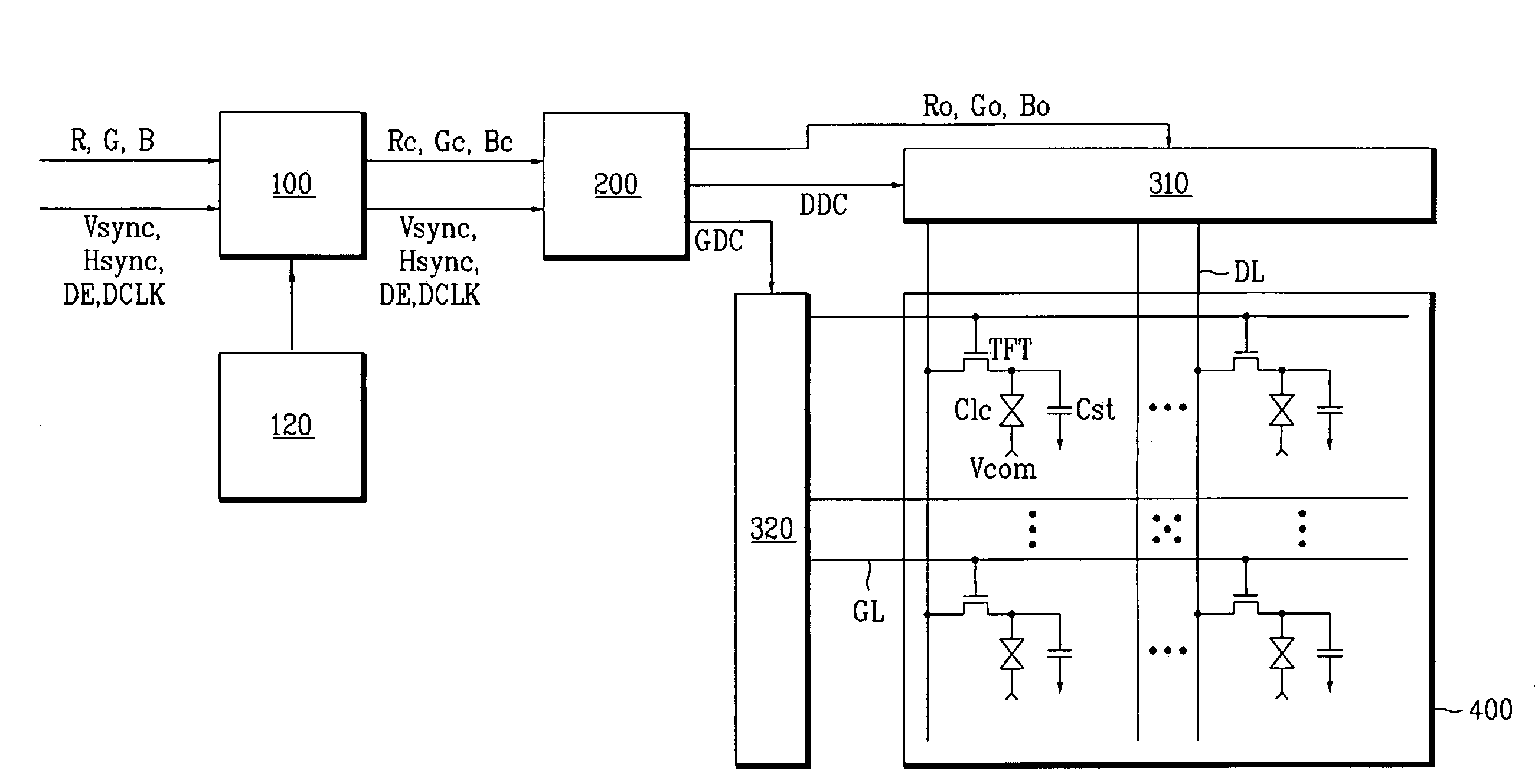
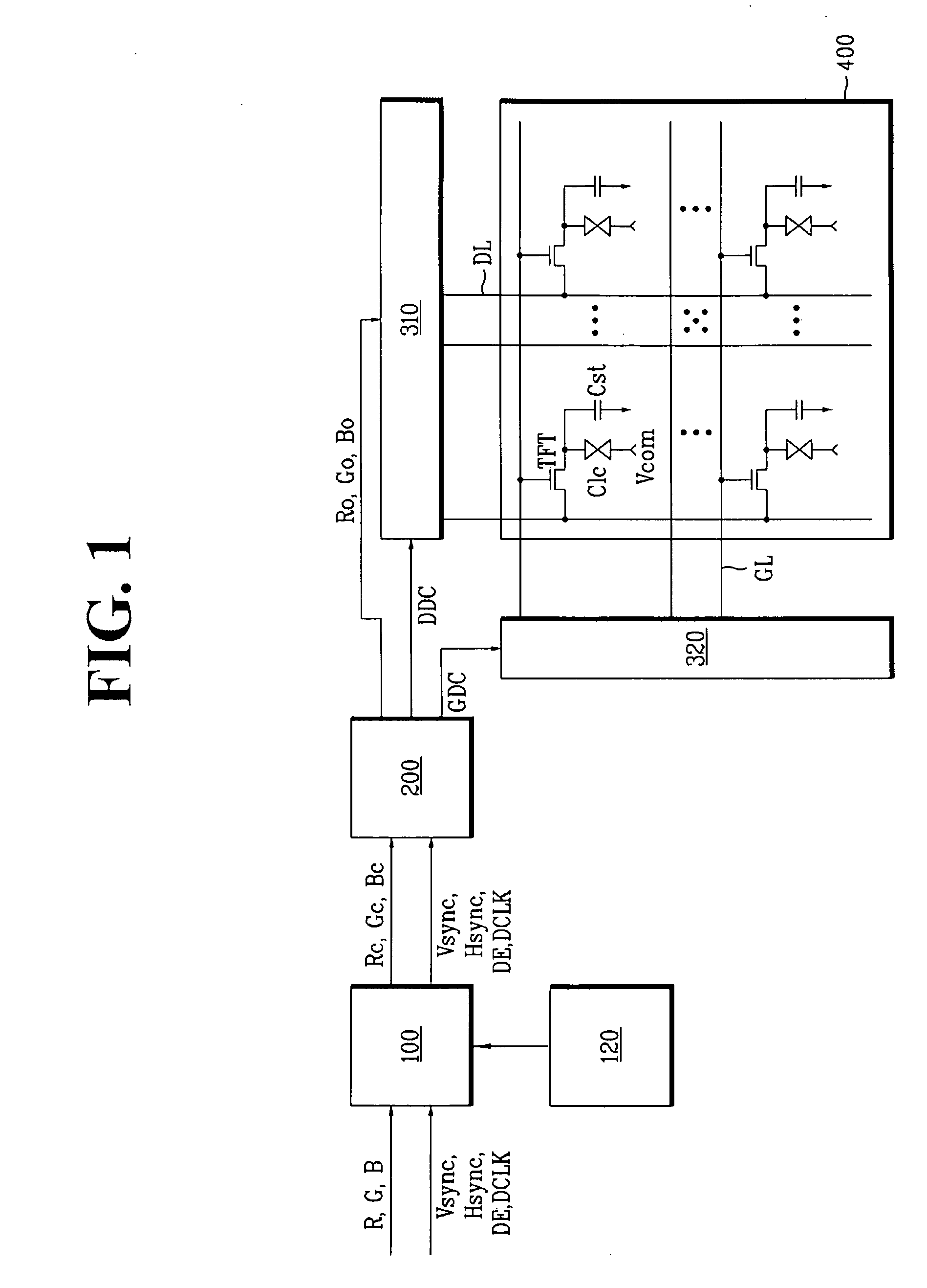
[0027]FIG. 1 illustrates a block diagram of a liquid crystal display device in accordance with a preferred embodiment of the present invention.

[0028]Referring to FIG. 1, the liquid crystal display device includes a compensation circuit 100, a timing controller 200, a data driver 310 and a gate driver 320 for driving a liquid crystal display panel 400, and a memory 120 connected to the compensation circuit 100. The compensation circuit 100 may be built-in the timing controller 200 to form a semiconductor chip.

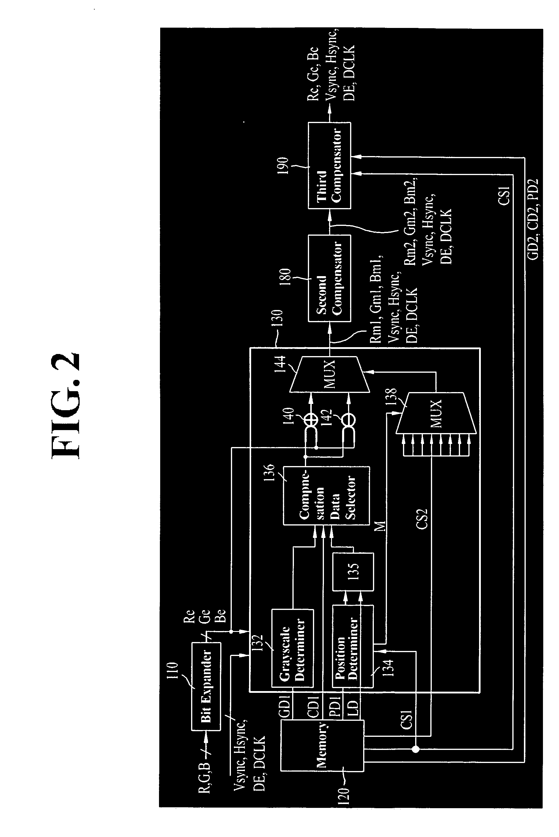
[0029]The memory 120 has regular patterned defect information stored therein, including position information PD1 on regular patterned defective regions, such as transverse lines and / or longitudinal lines...


PUM


Abstract

Circuit for compensating a display defect in a video display device of the present invention includes a memory having position information on a plurality of regular patterned defective regions of a display panel, gray scale section information, a defect level data on each of the regular patterned defective regions, and a plurality of compensation data on each of the defect level data stored therein, a first compensation unit, upon reception of data to be displayed on the regular patterned defective regions, for determining defect level data on the regular patterned defective regions of the data to be displayed, selecting a compensation data set on the defect level data determined thus, and selecting a compensation data on the data to be displayed from the compensation data selected thus, for compensating the data to be displayed, and a second compensator for distributing the data compensated thus at the first compensation unit spatially and temporally by using dither patterns for making fine compensation, thereby suppressing size increase of the compensation data.

Description

[0001]This application claims the benefit of the Patent Korean Application No. P2008-053079, filed on Jun. 5, 2008, which is hereby incorporated by reference for all purposes as if fully set forth herein.BACKGROUND OF THE INVENTION[0002]1. Field of the Invention[0003]The present invention relates to video display devices, and more particularly, to circuit and method for compensating a display defect in a video display device which can reduce a size of a memory which stores a compensation data on a plurality of regular patterned defective regions.[0004]2. Discussion of the Related Art[0005]Currently, as the video display devices, flat display devices, such as liquid crystal display device LCD, plasma display panel PDP, organic light emitting diode OLED, are used, mostly.[0006]The video display device passes through an inspection process for detecting a display defect after finishing fabrication of a display panel which displays a video. Though the display panel having the display def...

Claims


Application Information

Patent Timeline
IPC IPC(8): G06T1/60
CPCG09G3/20G09G3/2055G09G3/3648G09G2330/10G09G2320/0285G09G2330/08G09G2320/0233G02F1/133G02F1/13G09G3/36H04N5/21
Inventor HWANG, JONG HEEKIM, HYE JINPARK, JU SEONG
Owner LG DISPLAY CO LTD
Learn More