Integrated circuit

a technology of integrated circuits and integrated circuits, applied in the direction of diodes, basic electric elements, semiconductor devices, etc., can solve the problems of insufficient esd robustness and attenuation of high-frequency signals supplied to rf input pads, and achieve the effects of reducing impedance, reducing impedance, and minimizing the size of diodes

Inactive Publication Date: 2009-12-10
RENESAS ELECTRONICS CORP
View PDF5 Cites 16 Cited by
  • Summary
  • Abstract
  • Description
  • Claims
  • Application Information

AI Technical Summary

Benefits of technology

[0018]The integrated circuit according to the embodiment of the invention configures the clamp circuit in the input protection circuit cell. This makes it possible to provide more discharge paths for an ESD pulse current than conventional arts and reduce the impedance. The reduction in the impedance for the discharge path can minimize the

Problems solved by technology

There has been a problem that a high-frequency signal supplied to an RF input pad attenuates due to a large input capacitance from the diodes 1 and 2 of several picofarads

Method used


Image

  • Integrated circuit
  • Integrated circuit
  • Integrated circuit

Examples


Embodiment Construction

[0030]The following describes the invention with reference to the accompanying drawings showing embodiments.

[0031]

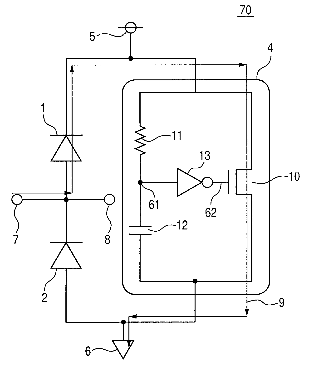
[0032]FIG. 5 shows a circuit diagram of the input protection circuit cell according to an embodiment of the invention.

[0033]An input protection circuit cell 70 is located between a signal pin of a mounted integrated circuit and an internal circuit including a high-frequency circuit. The input protection circuit cell 70 includes an input terminal 7 and an output terminal 8. The input terminal 7 is coupled to the signal pin. The output terminal 8 is coupled to the high-frequency circuit as well as the input terminal 7 and a node (coupling node) 60. A first diode 1 is provided between the node 60 and a high-voltage power supply (VDD) 5 and supplies an electric current from the node 60 to the VDD 5. A second diode 2 is provided between the node 60 and a low-voltage power supply (GND) 6 and supplies an electric current from the GND 6 to the node 60. Further, a clamp circuit 4...


PUM


Abstract

An integrated circuit aims to decrease a parasitic resistance between an input protection circuit cell and a power supply cell including a clamp circuit, restrain a size of a diode from increasing beyond ESD robustness of the diode itself in order to compensate for a decrease in the ESD robustness, and prevent high-frequency signal power from decreasing due to a large capacitance component from a diode in an input protection circuit and a parasitic resistance component from a series resistor. The input protection circuit cell includes: an input terminal coupled to a signal pin; an output terminal coupled to not only a high-frequency circuit but also the input terminal and a node; a diode that is provided between the node and VDD and makes an electric current flow from the node to VDD; another diode that is provided between the node and GND and makes an electric current flow from GND to the node; and a clamp circuit coupled between VDD and GND parallel to the diodes.

Description

CROSS-REFERENCE TO RELATED APPLICATIONS[0001]The disclosure of Japanese Patent Application No. 2008-149200 filed on Jun. 6, 2008 including the specification, drawings and abstract is incorporated herein by reference in its entirety.BACKGROUND OF THE INVENTION[0002]The present invention relates to an integrated circuit including an input protection circuit cell.[0003]FIG. 1 shows an input protection circuit cell 70 and a power supply cell 71 according to a conventional technology. To ensure ESD robustness, the input protection circuit cell 70 according to a conventional technology uses diodes 1 and 2. The diodes each have a capacitance of several picofarads and are reversely coupled between a power supply voltage (VDD) and a signal input line and between the signal input line and a ground (GND). A series resistor 40 is serially coupled to the signal input line. In a power supply cell 51, as shown in FIG. 1, an input circuit 43 and a clamp circuit 4 are parallel coupled between VDD an...

Claims


Application Information

Patent Timeline
IPC IPC(8): H02H9/00
CPCH01L23/60H01L27/0255H01L2223/6688H01L2924/3011H01L2924/0002H01L2924/00
Inventor SASAKI, NAGISA
Owner RENESAS ELECTRONICS CORP
Why Eureka
Try Eureka