Eureka AIR delivers breakthrough ideas for toughest innovation challenges, trusted by R&D personnel around the world.

Circuit and method for terminating data line of semiconductor integrated circuit

Inactive Publication Date: 2009-12-10
SK HYNIX INC
View PDF5 Cites 2 Cited by
  • Summary
  • Abstract
  • Description
  • Claims
  • Application Information

AI Technical Summary

Benefits of technology

[0009]a circuit and a method for terminating a data line of a semiconductor IC capable of improving data transmission rate and reducing cross talk characteristics are described herein.

Problems solved by technology

However, conventional semiconductor ICs are problematic that since the global data lines GIO swing between the ground voltage (VSS) level and the power supply voltage (VDD) level, the data transmission rate of the global data lines GIO is reduced due to the large resistance and capacitance.
In addition, since the global data lines GIO swing between the ground voltage (VSS) level and the power supply voltage (VDD) level, cross talk characteristics severely deteriorate between the adjacent lines.

Method used


Image

  • Circuit and method for terminating data line of semiconductor integrated circuit
  • Circuit and method for terminating data line of semiconductor integrated circuit
  • Circuit and method for terminating data line of semiconductor integrated circuit

Examples


Embodiment Construction

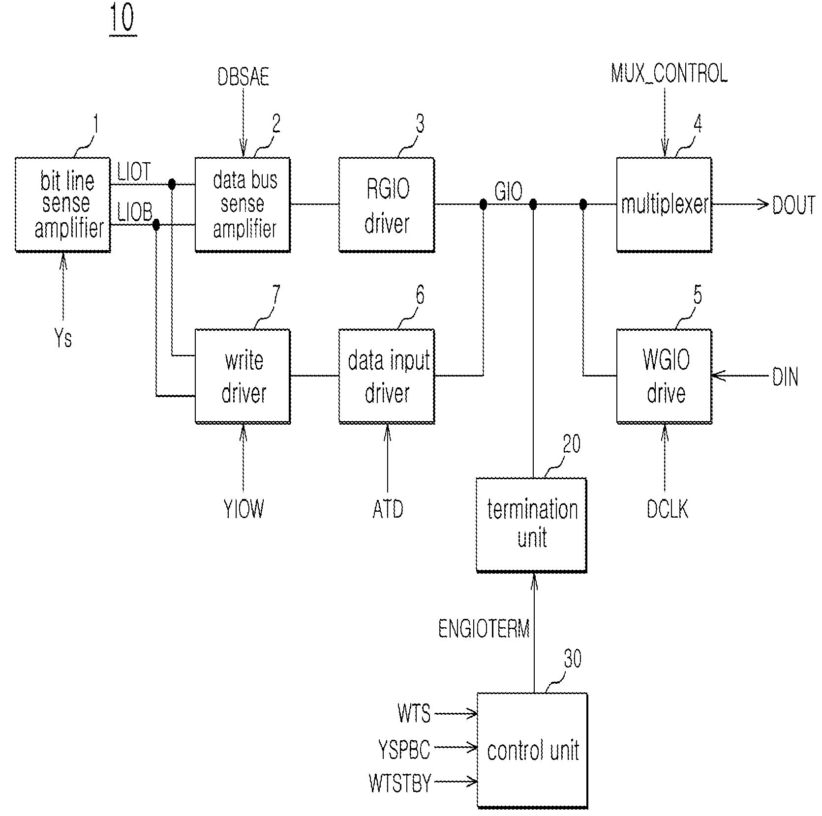
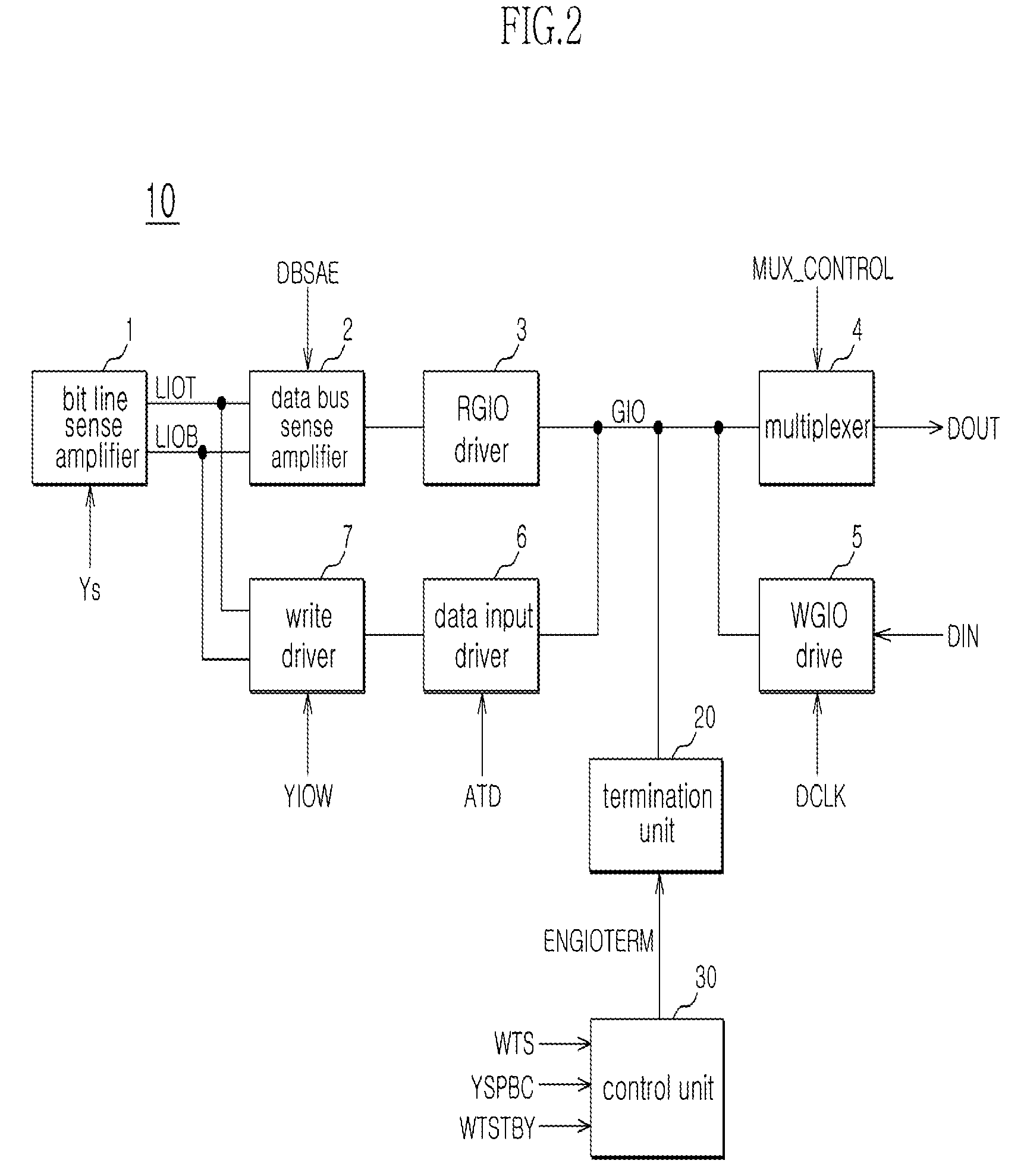
[0023]FIG. 2 is a schematic block diagram of an exemplary semiconductor IC according to one embodiment. In FIG. 2, a semiconductor IC can be configured to include a bit line sense amplifier 1, a data bus sense amplifier 2, a RGIO driver 3, a multiplexer 4, a WGIO drive 5, a data input driver 6, a write driver 7, a global data line GIO, a termination unit 20, and a control unit 30.

[0024]The bit line sense amplifier 1, which can be coupled between a memory cell of a core block and local data lines LIOT and LIOB, can sense and amplify input data signal when a column select signal ‘YS’ is activated. The data bus sense amplifier 2 can sense and amplify the data loaded on the local data lines LIOT and LIOB according to an enable signal ‘DBSAE’ at a read operation. The RGIO driver 3 can drive the global data line GIO at a voltage level, which can be correspondent to an output signal of the data bus sense amplifier 2, at the read operation.

[0025]At the read operation, the multiplexer 4 can ...


PUM


Abstract

A data line termination circuit in a semiconductor integrated circuit includes a data line, a control unit for generating a termination control signal activated during a time section that includes a driving section in which data is driven to the data line, and a termination unit for terminating the data line to a predetermined voltage level in response to the termination control signal

Description

CROSS-REFERENCES TO RELATED APPLICATION[0001]The present application claims priority under 35 U.S.C. §119(a) to Korean application number 10-2008-0052703, filed on Jun. 4, 2008, in the Korean Intellectual Property Office, which is incorporated herein by reference in its entirety as set forth in full.BACKGROUND[0002]1. Technical Field[0003]The embodiments described herein relate to a semiconductor integrated circuit (IC) and, more particularly, to a circuit having a terminated data line of a semiconductor IC and a method for terminating a data line of a semiconductor IC.[0004]2. Related Art[0005]FIG. 1 is a timing chart representing a conventional write operation in a semiconductor IC. In FIG. 1, when write command signals are sequentially applied to a semiconductor IC, data is input and arranged after a write latency (WL). In addition, a data clock signal ‘DCLK’ is issued in synchronization with a clock signal ‘CLK’ that is first generated after a time interval which is corresponden...

Claims


Application Information

Patent Timeline
IPC IPC(8): G11C7/00G11C5/14G11C8/18G11C8/00
CPCG11C7/1048G11C7/1051G11C7/1078G11C7/22G11C8/18H03K19/0175
Inventor KU, KIE BONG
Owner SK HYNIX INC
Why Eureka
Eureka Blog
Learn More