
Protection circuit, and semiconductor device and light emitting device using such protection circuit

a protection circuit and circuit technology, applied in emergency protection circuit arrangements, emergency protection circuit arrangements for limiting excess voltage/current, transistors, etc., can solve problems such as reliability and voltage output of batteries, and achieve the effect of raising the reliability of semiconductor devices

Inactive Publication Date: 2009-12-17
ROHM CO LTD
View PDF3 Cites 0 Cited by
  • Summary
  • Abstract
  • Description
  • Claims
  • Application Information

AI Technical Summary

Benefits of technology

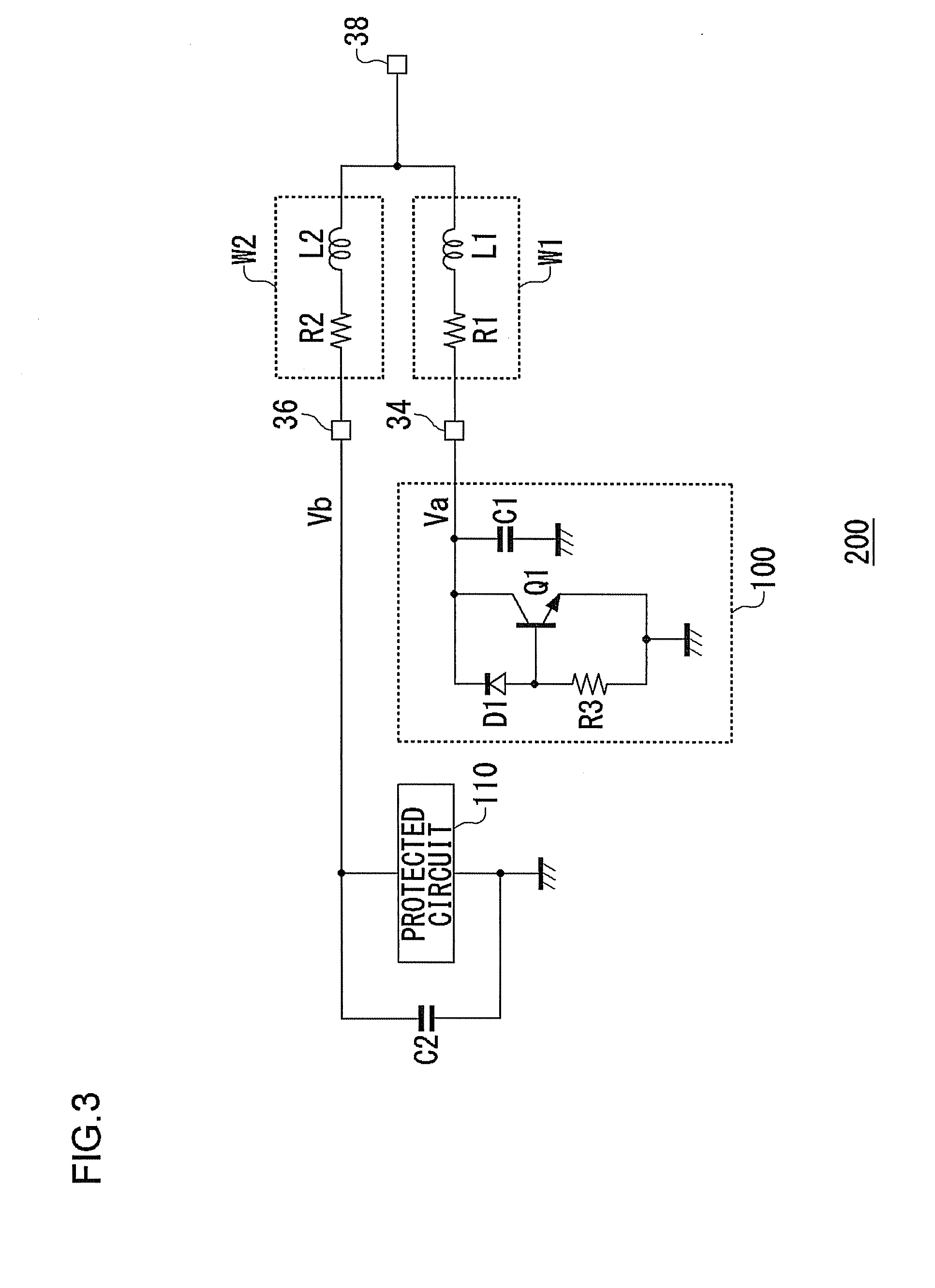
[0024]According to the embodiment, when a surge voltage occurs, a current due to the second transistor in addition to the first transistor is extracted. As a result, since a current is extracted from both ends of a wire including the significant inductance component, LCR oscillation can be suppressed, and voltage oscillation can be suppressed.
[0028]By the size of the first and the second transistors being approximately the same, electrical current amount extracted by each of the transistors can be made approximately equal, and it is possible to suppress oscillation.
[0031]According to this embodiment, the driver circuit can be protected from a surge voltage and the like, and it is possible to raise reliability of the semiconductor device.

Problems solved by technology

Since voltage outputted from the battery 20 is unstable, for a semiconductor integrated circuit used for this type of application, reliability is required particularly against surge voltages and the like.

Method used


Image

  • Protection circuit, and semiconductor device and light emitting device using such protection circuit
  • Protection circuit, and semiconductor device and light emitting device using such protection circuit
  • Protection circuit, and semiconductor device and light emitting device using such protection circuit

Examples


Embodiment Construction

[0041]The invention will now be described based on preferred embodiments which do not intend to limit the scope of the present invention but exemplify the invention. All of the features and the combinations thereof described in the embodiment are not necessarily essential to the invention.

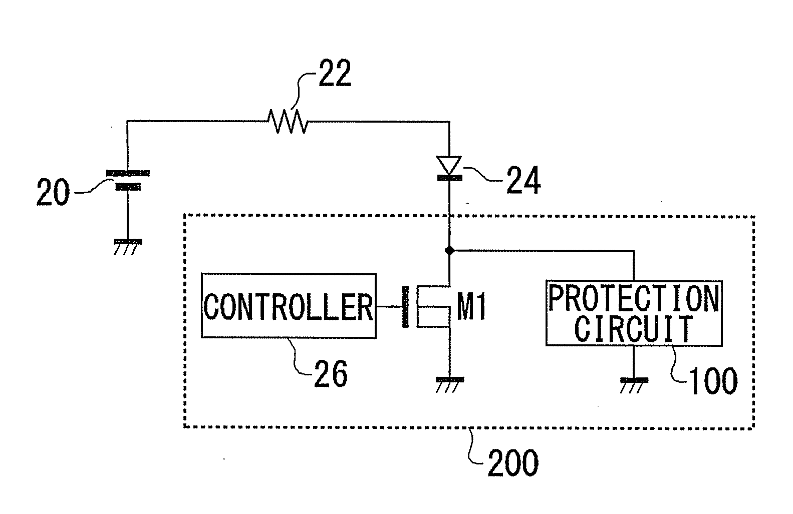
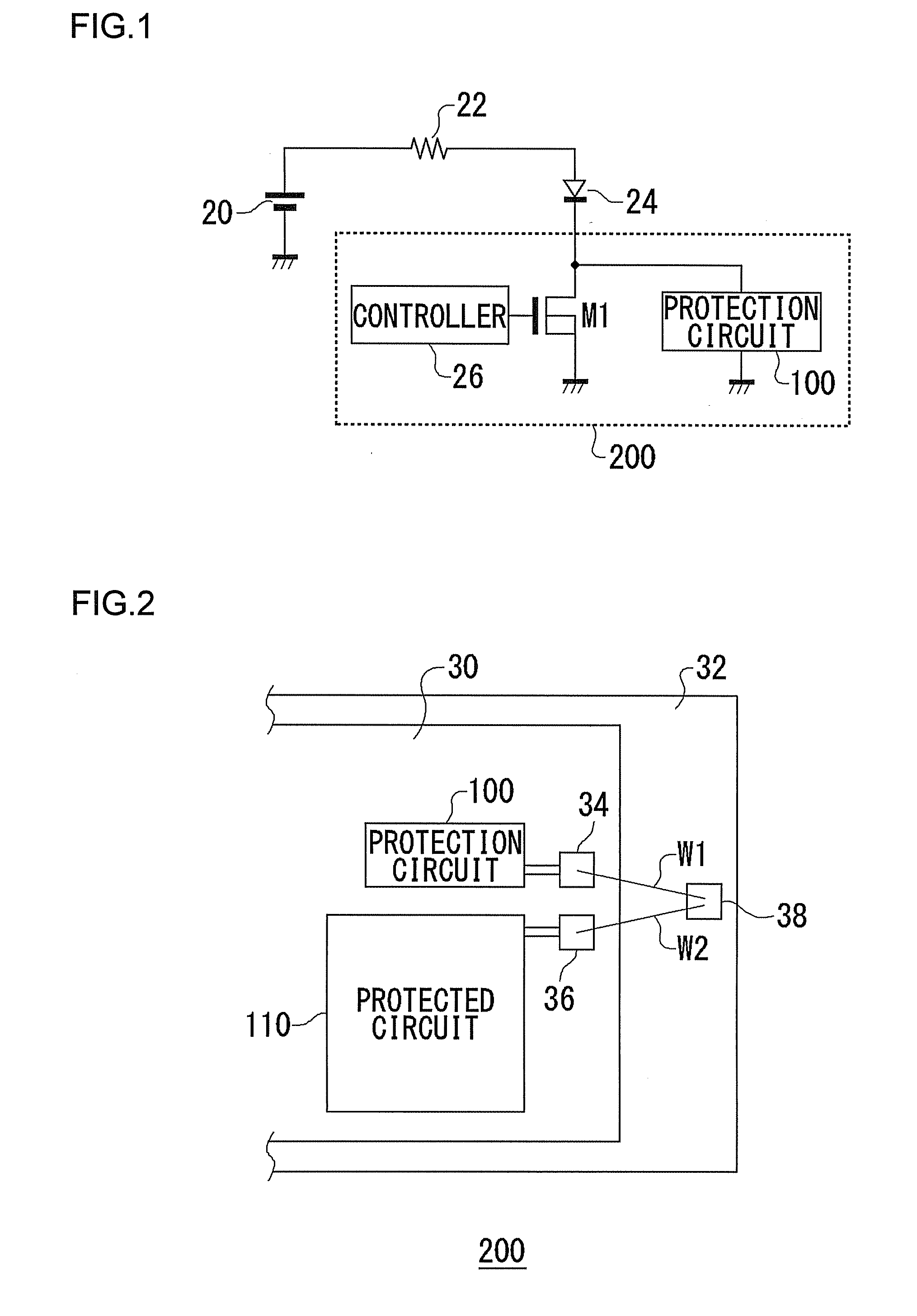
[0042]A protection circuit 100 according to the present embodiment is used, for example, in an LED driver circuit 200 described in FIG. 1. As shown in FIG. 2, also in the present embodiment, the protection circuit 100 and a protected circuit 110, that is to be protected, are integrated on the same semiconductor substrate 30, and the protection circuit 100 and the protected circuit 110 are respectively provided with bonding pads 34 and 36.

[0043]The bonding pads 34 and 36 are connected by bonding wires W1 and W2 that are lines including significant inductance components, via a bonding pad 38 arranged on a base 32, on which the semiconductor substrate 30 is mounted.

[0044]FIG. 5 is a circuit diagram sh...


PUM


Abstract

In a protection circuit connected, via lines including an inductance component, to a circuit to be protected, a first transistor is arranged on a path to ground from a connection point of the protection circuit and the line. A second transistor is arranged on a path to ground from a connection point of the circuit to be protected and the line, and extracts, from a connection point, a current corresponding to a current flowing in the first transistor. The first and the second transistors are NPN bipolar transistors having a base and an emitter are commonly connected. A resistor is connected between the base and the emitter of the first transistor, and a diode is connected between the base and a collector.

Description

BACKGROUND OF THE INVENTION[0001]1. Field of the Invention[0002]The present invention relates to circuit protection technology for protecting a circuit to be protected, from surge voltages and the like.[0003]2. Description of the Related Art[0004]Many semiconductor integrated circuits are used in various electronic devices, starting from mobile telephones, PDAs (Personal Digital Assistants), and laptop personal computers, or electrical systems in automobiles. Since usage in all kinds of conditions is envisaged for such semiconductor integrated circuits, high reliability is required. In order to improve reliability, in general, a protection circuit is provided for each bonding pad of an input-output terminal connected to the outside of a circuit.[0005]Among such protection circuits, a voltage clamp circuit may be provided so that the reliability of an internal circuit that is to be protected (referred to as a protected circuit, below), does not deteriorate, even in cases in which a s...

Claims


Application Information

Patent Timeline
IPC IPC(8): H01L33/00H01L29/73H01L21/822H01L27/04H02H9/00
CPCH01L27/0248H05B33/0884Y02B20/341H01L2224/48227H01L2224/49113H01L2924/1305H01L2924/30107H01L2924/00H05B45/50Y02B20/30
Inventor OKAZAKI, MITSURUTAKAHASHI, NAOKISHIMIZU, AKIRANAKATA, KENICHI
Owner ROHM CO LTD
Learn More