Method, design structures, and systems for current mode logic (CML) differential driver ESD protection circuitry

a protection circuit and differential driver technology, applied in the direction of circuit arrangements, overvoltage protection resistors, emergency protection arrangements for limiting excess voltage/current, etc., can solve the problems of esd failure, driver nfets failure in the topology of the cml driver, and is susceptible to electrostatic discharge stress

Inactive Publication Date: 2009-12-17
IBM CORP
View PDF7 Cites 11 Cited by
  • Summary
  • Abstract
  • Description
  • Claims
  • Application Information

AI Technical Summary

Benefits of technology

[0011]As a result of the summarized invention, technically we have achieved a solution for forming an integrated circuit having an ESD protection scheme.

Problems solved by technology

The lower breakdown voltage of the devices makes them susceptible to the electrostatic discharge (ESD) stress.
This current can exceed the current limit of the salicided driver transistor, leading to failures.
Recently, driver NFETs failure was discovered in the CML driver topology during pad-to-pad or pin-to-pin electrostatic discharge (ESD) stress.
This causes drain-source short on the partner driver transistor, leading to ESD failures.

Method used


Image

  • Method, design structures, and systems for current mode logic (CML) differential driver ESD protection circuitry
  • Method, design structures, and systems for current mode logic (CML) differential driver ESD protection circuitry
  • Method, design structures, and systems for current mode logic (CML) differential driver ESD protection circuitry

Examples


Embodiment Construction

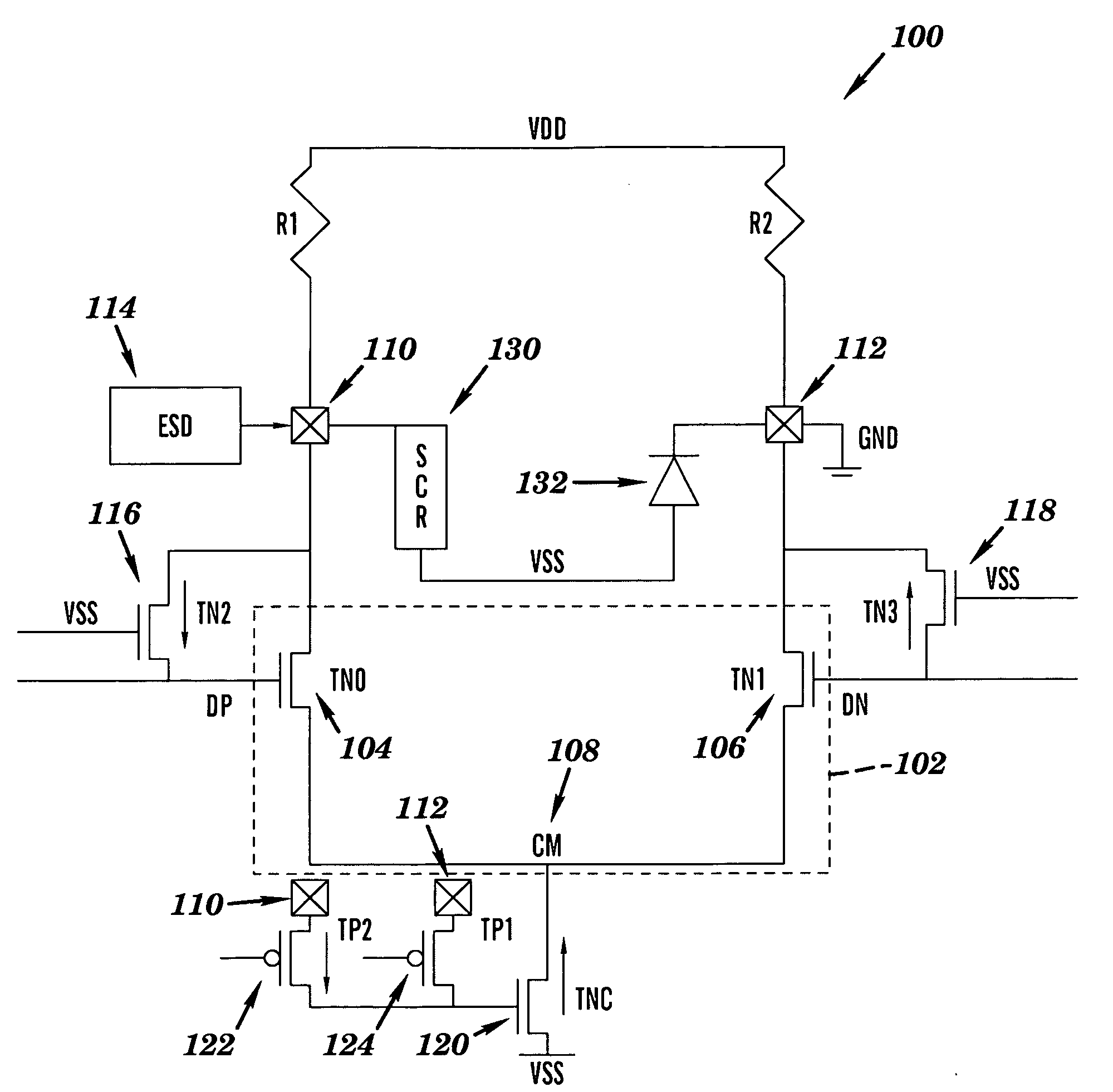
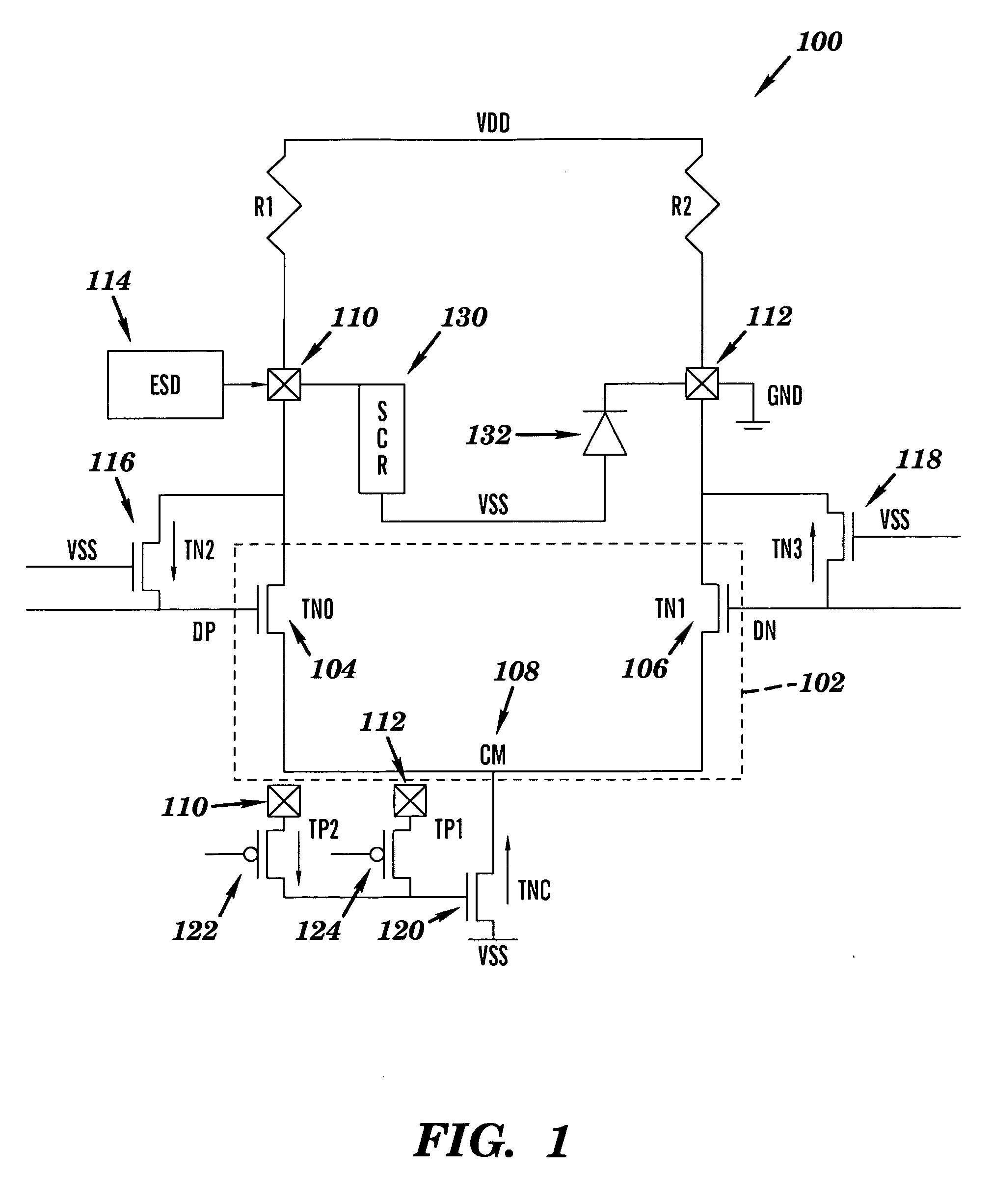
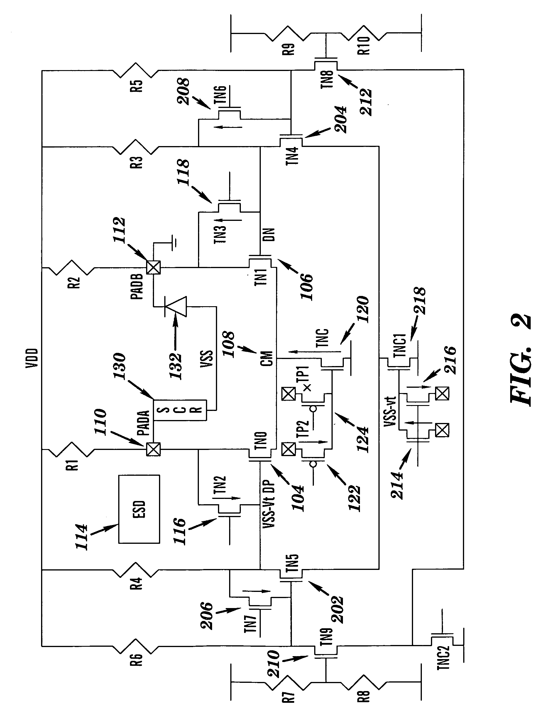
[0017]The present invention and the various features and advantageous details thereof are explained more fully with reference to the non-limiting embodiments that are illustrated in the accompany drawings and detailed in the following description. Descriptions of well-known or conventional components and processing techniques are omitted so as to not necessarily obscure the present invention in detail. The examples used herein are intended merely to facilitate an understanding of ways in which the invention may be practiced and to further enable those of skill in the art to practice the invention. Accordingly, the examples should not be construed as limiting the scope of the invention.

[0018]The inventors herein have recognized an electrostatic discharge (ESD) protection circuit scheme for differential driver pin-to-pin ESD stress. The inventors herein have recognized that using switches to turn off driver transistors and switches to turn-off pre-driver transistors, if any, will enha...


PUM


Abstract

A hardware description language (HDL) design structure encoded on a machine readable data storage medium, the HDL design comprising elements that when processed in a computer aided design system generates a machine executable representation of a device for implementing dynamic refresh protocols for DRAM based cache. The HDL design structure further comprises an integrated circuit having a differential driver, comprising: a first driver and a second driver forming the differential driver, the drivers are coupled in parallel between a first voltage source and a second voltage source; a first switch coupled to the first driver and configured to turn off the first driver during an ESD event such that the first driver sustains stress during the ESD event; and a second switch coupled to the second driver and configured to turn off the second driver during the ESD event such that the second driver sustains stress during the ESD event.

Description

BACKGROUND OF THE INVENTION[0001]1. Field of the Invention[0002]This invention relates to systems, methods, and design structures for current mode logic differential driver ESD protection circuitry.[0003]2. Description of Background[0004]For high-speed differential operation in the GHz range, current mode logic (CML) drivers are typically used for their large attainable bandwidth. These are simple resistively loaded differential amplifiers.[0005]As technology scales supply voltage, transistor threshold voltage, breakdown voltage reduces. The lower breakdown voltage of the devices makes them susceptible to the electrostatic discharge (ESD) stress. Lower threshold voltages of the transistors make them conduct large current at small overdrive voltages. This current can exceed the current limit of the salicided driver transistor, leading to failures.[0006]Recently, driver NFETs failure was discovered in the CML driver topology during pad-to-pad or pin-to-pin electrostatic discharge (ESD...

Claims


Application Information

Patent Timeline
Patent Type & Authority Applications(United States)
IPC IPC(8): H02H9/00
CPCH01L27/0251H03F1/52H03F1/523H03F2203/45504H03F2203/45466H03F2203/45486H03F3/45188
Inventor GAUTHIER, JR., ROBERT J.LI, JUNJUNSRIVASTAVA, ANKIT
Owner IBM CORP
Why Eureka
Try Eureka