Capacitance type input device and display device with input function

a display device and input function technology, applied in the field of capacitive type input device and display device with input function, can solve the problems of weak time variation, narrow operation temperature range, resistance film input device, etc., and achieve the effect of simple configuration

Active Publication Date: 2009-12-24
JAPAN DISPLAY WEST
View PDF3 Cites 640 Cited by
  • Summary
  • Abstract
  • Description
  • Claims
  • Application Information

AI Technical Summary

Benefits of technology

[0011]An advantage of some aspects of the invention is that it provides a capacitance type input device capable of making a light transmission electrode pattern on a light transmission substrate inconspicuous by a simple configuration, and a display device with an input function.

Problems solved by technology

Since the resistance film type input device has a double sheet structure including a film and glass and a structure in which a film is pressed to short-circuit, the resistance film type input device has problems such as a narrow operation temperature range and weak time variation.
However, if a region in which the light transmission electrode patterns or the like are formed and a region in which the light transmission electrode patterns or the like are not formed are significantly different from each other in reflectivity, the existence of the light transmission electrode patterns is unpreferably conspicuous.
Therefore, the existence of the first light transmission electrodes and the second light transmission electrodes is inconspicuous.
Therefore, the existence of the crossing portions is inconspicuous when being viewed from the input surface side.

Method used


Image

  • Capacitance type input device and display device with input function
  • Capacitance type input device and display device with input function
  • Capacitance type input device and display device with input function

Examples


embodiment 1

Whole Configuration

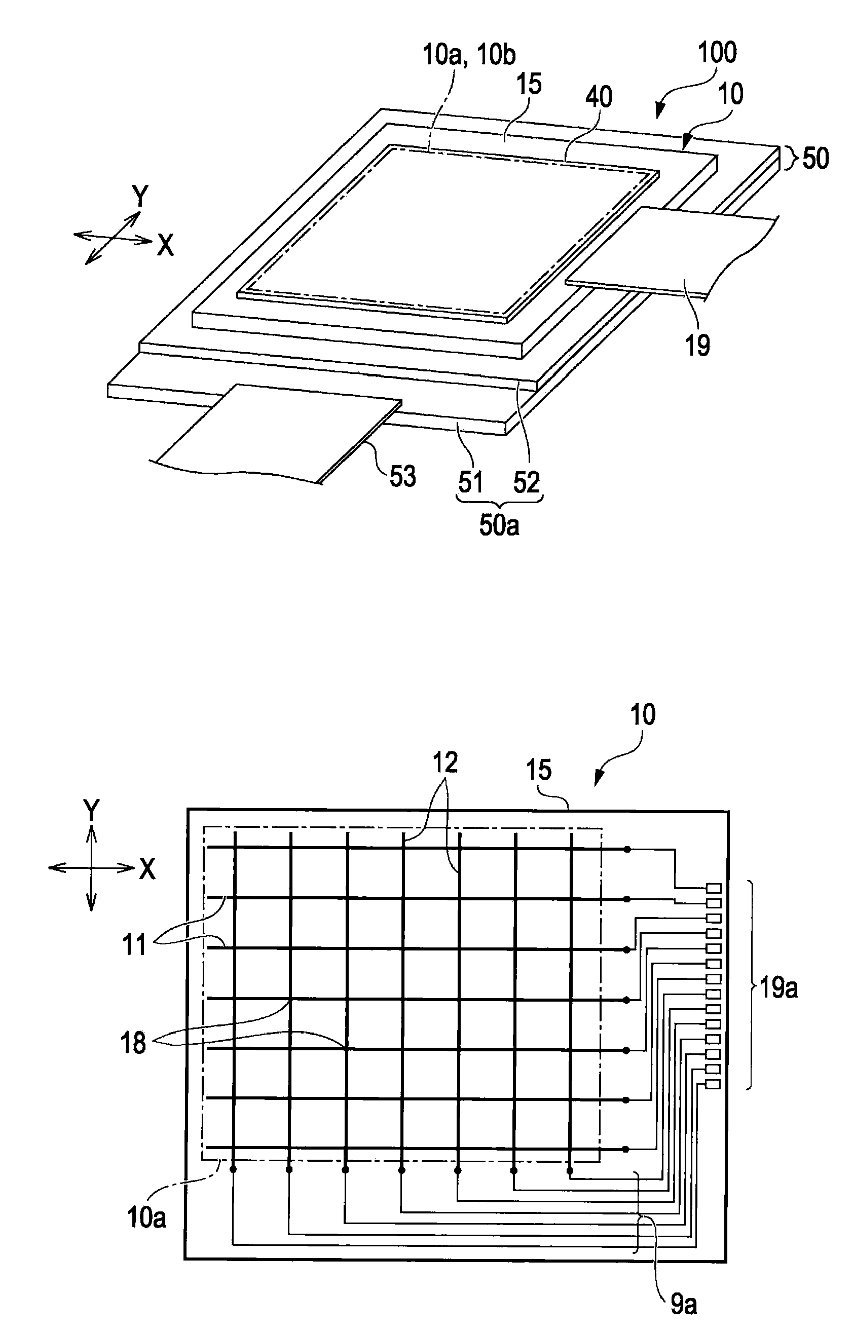
[0038]FIGS. 1A and 1B are explanation views schematically showing the configuration of a display device with an input device according to the invention and an explanation view schematically showing the planar configuration of the display device with the input device, respectively. In FIG. 1B, first light transmission electrode patterns and second light transmission electrode patterns are simplified by a solid line and the number of electrode patterns is reduced.

[0039]In FIG. 1A, a display device 100 with an input device according to the present embodiment generally includes a liquid crystal device 50 as an image generating device and an input device 10 (touch panel) which has a panel shape and is arranged so as to be overlapped on a display light emitting side surface of the liquid crystal device 50. The liquid crystal device 50 includes a transmissive type, reflective type, or transflective type active matrix liquid crystal panel 50a. In a transmissive type or tr...

embodiment 2

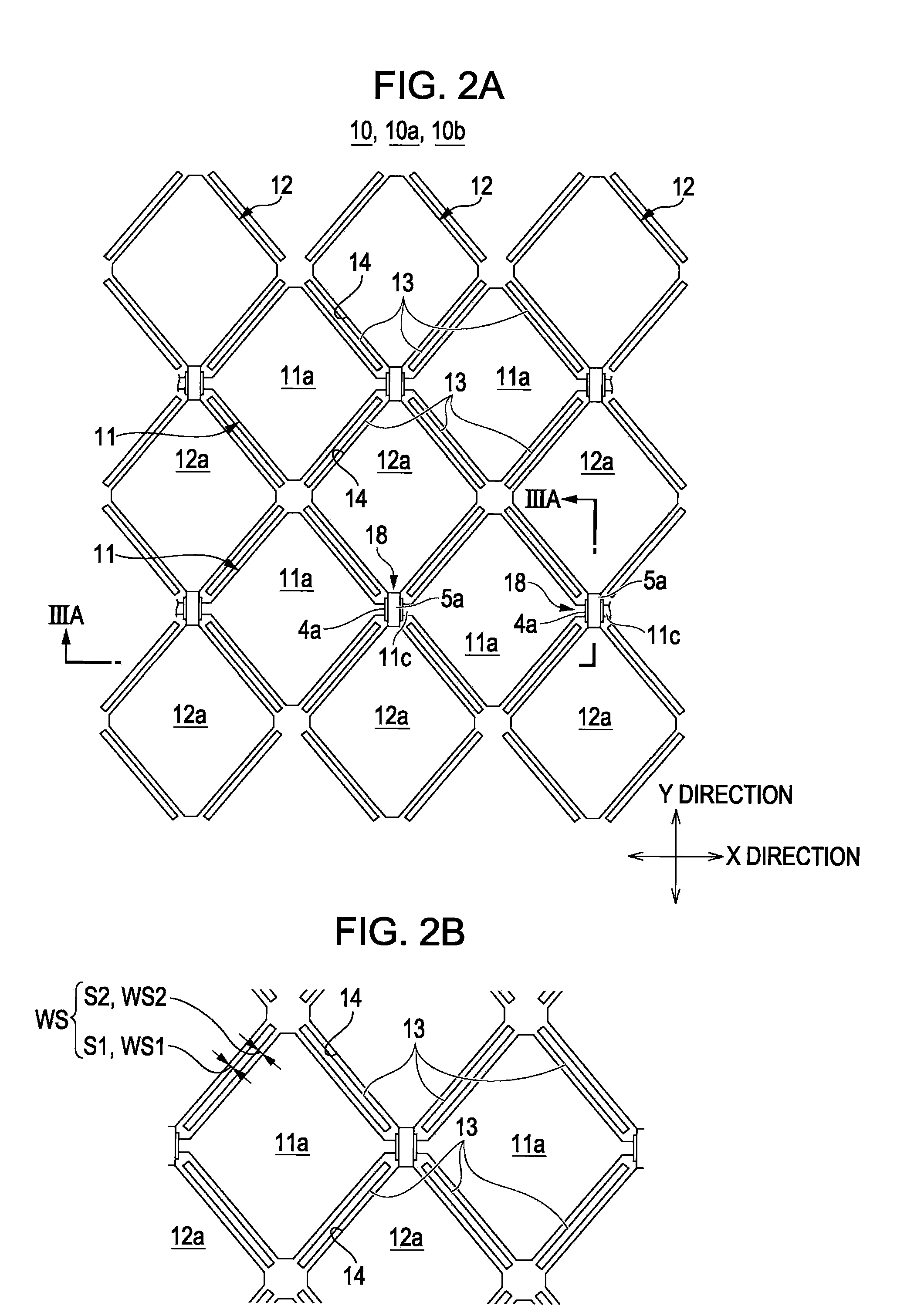
[0072]FIG. 5 is an explanation view showing the planar configuration of first light transmission electrode patterns and second light transmission electrode patterns formed in an input device according to Embodiment 2 of the invention. FIGS. 6A and 6B are cross-sectional views taken along line VIA-VIA of FIG. 5 according to Embodiment 2 of the invention and a cross-sectional view showing a connection structure of light transmission electrode patterns and metal wires, respectively. Since the basic configuration of the present embodiment is equal to that of Embodiment 1, the same portions are denoted by the same reference numerals and the description thereof will be omitted.

[0073]In FIGS. 5 and 6A, the input device 10 according to the present embodiment is a capacitance type touch panel like Embodiment 1, and, in an input surface 10b of a light transmission substrate 15, a plurality of rows of first light transmission electrode patterns 11 extending in a first direction and a plurality...

embodiment 3

[0085]FIG. 8 is an explanation view showing the planar configuration of first light transmission electrode patterns and second light transmission electrode patterns formed in an input device according to Embodiment 3 of the invention. FIGS. 9A and 9B are cross-sectional views taken along line IXA-IXA of FIG. 8 according to Embodiment 3 of the invention and a cross-sectional view showing a connection structure of a light transmission electrode pattern and a metal wire, respectively. Since the basic configuration of the present embodiment is equal to that of Embodiment 1, the same portions are denoted by the same reference numerals and the description thereof will be omitted.

[0086]In FIGS. 8 and 9A, the input device 10 according to the present embodiment is a capacitance type touch panel like Embodiment 1, and, in an input surface 10b of a light transmission substrate 15, a plurality of rows of first light transmission electrode patterns 11 extending in a first direction and a plurali...


PUM


Abstract

Provided is a capacitance type input device, in which a plurality of first light transmission electrodes extending in a first direction and a plurality of second light transmission electrodes extending in a second direction crossing the first direction are formed in an input region of a light transmission substrate, wherein, when the light transmission substrate is viewed from the top, dummy patterns formed of the same light transmission conductive film as the first light transmission electrodes and the second light transmission electrodes are formed in regions sandwiched between the first light transmission electrodes and the second light transmission electrodes.

Description

[0001]The entire disclosure of Japanese Patent Application No. 2008-158834, filed Jun. 18, 2008 is expressly incorporated by reference herein.BACKGROUND[0002]1. Technical Field[0003]The present invention relates to a capacitance type input device capable of detecting an approach position of a finger by a capacitance variation and a display device with an input function, which includes the capacitance type input device.[0004]2. Related Art[0005]In electronic apparatuses such as mobile telephones, car navigation systems, personal computers, ticket vending machines, bank terminals or the like, recently, there is provided an electronic apparatus in which a tablet input device is arranged on a surface of a liquid crystal device or the like, and a finger or the like is brought into contact with a place where a pointed image is displayed, while referring to the pointed image displayed in an image display region of the liquid crystal device, so as to input information corresponding to the p...

Claims


Application Information

Patent Timeline
Patent Type & Authority Applications(United States)
IPC IPC(8): G06F3/045
CPCG06F3/0412G06F2203/04111G06F3/044G06F3/0446G06F3/0443G06F3/0448G06F2203/04804
Inventor MATSUO, MUTSUMI
Owner JAPAN DISPLAY WEST
Why Eureka
Try Eureka