Photoelectric conversion device module and manufacturing method of the photoelectric conversion device module

a technology of photoelectric conversion device and conversion device module, which is applied in the manufacture of final products, pv power plants, basic electric elements, etc., can solve the problems of multi-layer junction type photoelectric conversion device module, difficult to form and inability to integrate photoelectric conversion cells using single-crystal silicon thin film on one substrate, etc., to achieve improved photoelectric conversion efficiency, excellent photoelectric conversion characteristics, and improved efficiency

Inactive Publication Date: 2009-12-31
SEMICON ENERGY LAB CO LTD
View PDF20 Cites 62 Cited by
  • Summary
  • Abstract
  • Description
  • Claims
  • Application Information

AI Technical Summary

Benefits of technology

[0033]According to one embodiment of the present invention, a manufacturing method of a novel photoelectric conversion device and a novel photoelectric conversion device module in which multi junction type photoelectric conversion devices are integrated is provided. In each of the multi junction type photoelectric conversion devices, a cell including a single-crystal semiconductor layer and a cell including a non-single-crystal semiconductor layer are stacked. Alternatively, a resource-saving photoe...

Problems solved by technology

However, because it is difficult to form a single-crystal silicon thin film by a method of the above-described deposition methods, integration of photoelectric conversion cells using a single-crystal silicon thin film on one substrate have...

Method used


Image

  • Photoelectric conversion device module and manufacturing method of the photoelectric conversion device module
  • Photoelectric conversion device module and manufacturing method of the photoelectric conversion device module
  • Photoelectric conversion device module and manufacturing method of the photoelectric conversion device module

Examples


embodiment 1

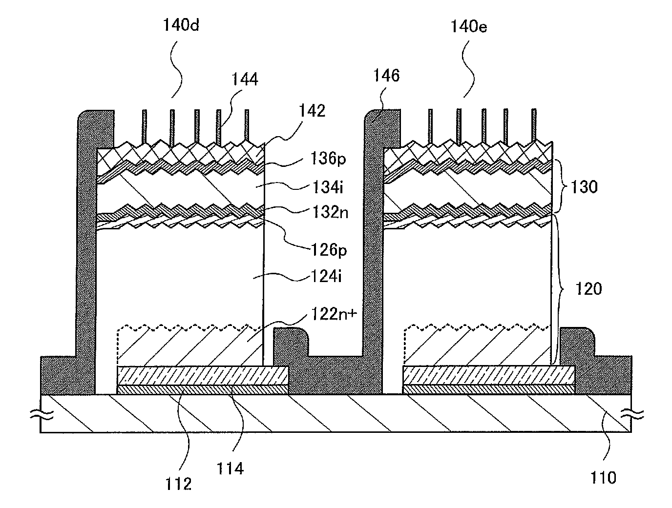
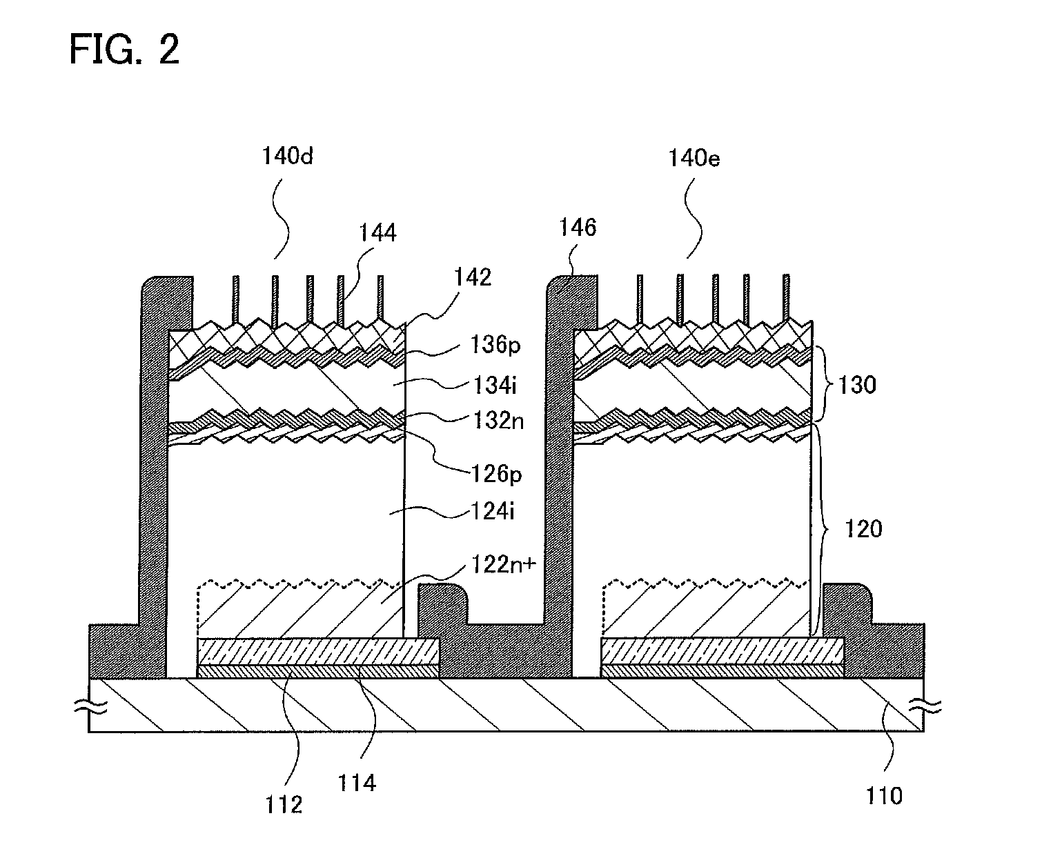
[0055]One mode of the present invention is a photoelectric conversion device module including, over one substrate, a plurality of photoelectric conversion cells (photoelectric conversion devices) in which a cell including a single-crystal semiconductor layer and a cell including a non-single-crystal semiconductor layer are stacked. The stack of the cell including a single-crystal semiconductor layer and the cell including a non-single-crystal semiconductor layer forms a multiple junction.

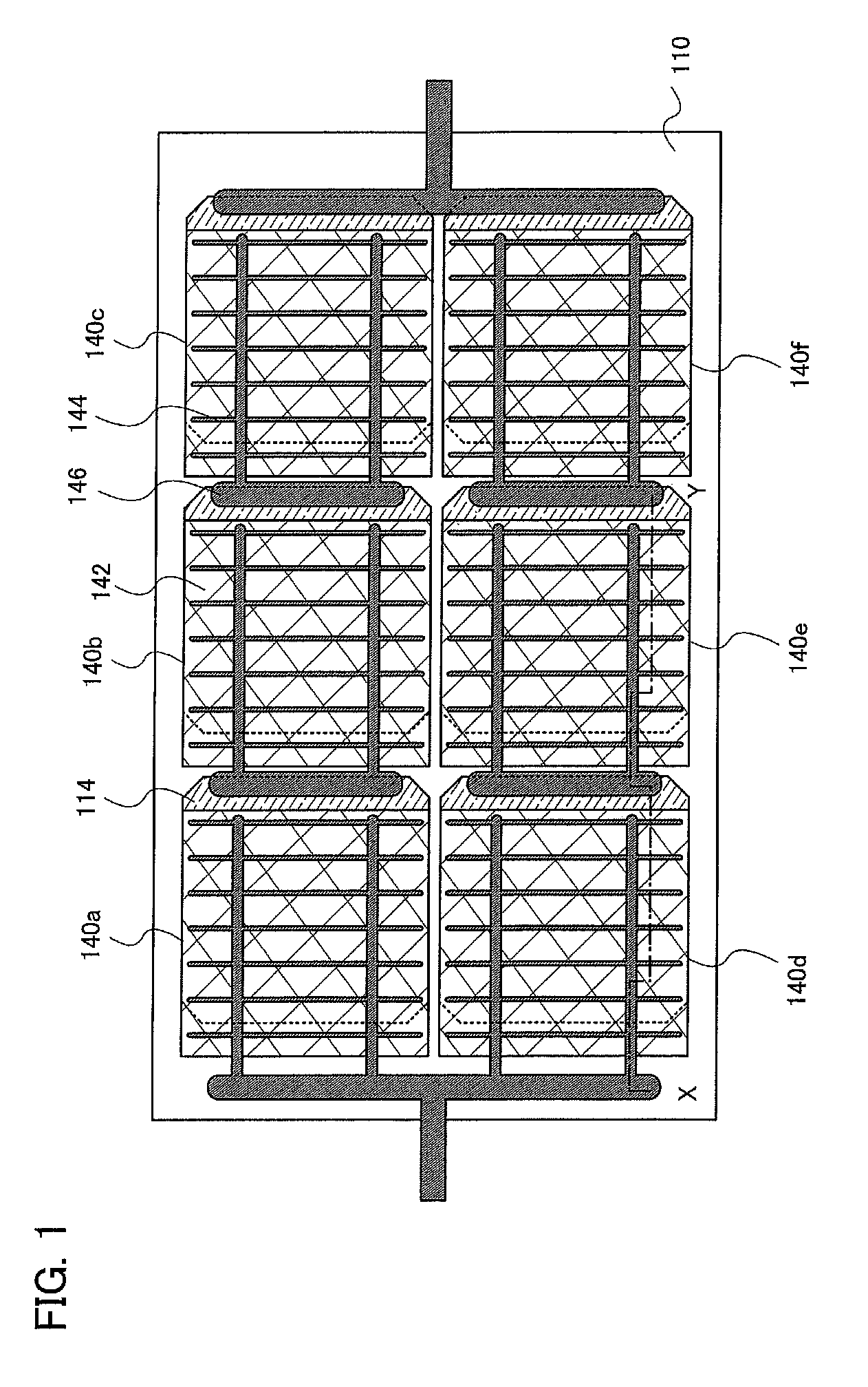
[0056]FIG. 1 is a schematic planar view of a photoelectric conversion device module in which a plurality of photoelectric conversion cells are provided over one substrate and are connected in series and / or in parallel. In addition, FIG. 2 illustrates a cross-sectional schematic view taken along the section line X-Y in FIG. 1. In this case is illustrated an example in which a plurality of planar photoelectric conversion devices are arranged over the one substrate having an insulating surface with a p...

embodiment 2

[0179]In this embodiment, an example of a method of manufacturing a photoelectric conversion device and a photoelectric conversion device module, which are different from that in the above embodiment, will be described. Note that description for the same parts as those of the above embodiment is omitted or partly simplified.

[0180]In the example of Embodiment 1, the n-type single-crystal semiconductor layer sliced from the n+ type semiconductor substrate is formed and the n+ type single-crystal semiconductor layer itself serves as the first impurity semiconductor layer 122n+. This embodiment describes an example, in which an n-type single-crystal semiconductor substrate is applied instead of the n+ type single-crystal semiconductor substrate.

[0181]As the single-crystal semiconductor substrate 101, an n-type single-crystal semiconductor substrate is prepared (FIG. 14A).

[0182]The embrittlement layer 105 is formed in a region at a predetermined depth from one surface of the single-cryst...

embodiment 3

[0192]In this embodiment, an example of a method of manufacturing a photoelectric conversion device and a photoelectric conversion device module, which are different from that in the above embodiment, will be described. Specifically, a method for forming a modified region to serve as an embrittlement layer in a single-crystal semiconductor substrate with use of multiphoton absorption is described. Note that description for the same parts as those of the above embodiment is omitted or partly simplified.

[0193]As illustrated in FIG. 15, a laser beam 230 is condensed inside the single-crystal semiconductor substrate 101 from the side of the surface on which the insulating layer 203 is formed. By scanning the single-crystal semiconductor substrate 101 with the laser beam 230, a modified region 205 is formed in a region at a predetermined depth of the single-crystal semiconductor substrate 101. A laser beam that allows multiphoton absorption is applied as the laser beam 230 and the focal ...


PUM


Abstract

A manufacturing method of a photoelectric conversion device module, wherein an insulating layer and a first electrode are formed over a base substrate; a plurality of single-crystal semiconductor substrates having a first conductivity type including embrittlement layers formed inside are attached; the plurality of single-crystal semiconductor substrates are separated at the embrittlement layers so that a plurality of stacked bodies including the insulating layer, the first electrode and a first single-crystal semiconductor layer is formed; a second single-crystal semiconductor layer is formed over the stacked bodies to form a first photoelectric conversion layer; a second photoelectric conversion layer including a non-single-crystal semiconductor layer is formed; a second electrode is formed; and selective etching is conducted to form photoelectric conversion cells which are element-separated, and a connecting electrode is formed to connect the second electrode of one photoelectric conversion cell and the first electrode of the other photoelectric conversion cell.

Description

BACKGROUND OF THE INVENTION[0001]1. Field of the Invention[0002]The present invention relates to a photoelectric conversion device module including a plurality of photoelectric conversion devices on one substrate and a manufacturing method of the photoelectric conversion device module.[0003]2. Description of the Related Art[0004]The progress of global warming is serious and there is a demand for clean energy. Photoelectric conversion devices typified by solar cells are thought to be typical of the next generation energy, and recent research and development has been extremely actively made and the market for solar cells are rapidly expanding.[0005]Solar light which is an energy source of a photoelectric conversion device is inexhaustible, available for free, has a possibility to contribute to reduction of carbon-dioxide emissions, and thus is very attractive. However, such a photoelectric conversion device using solar light cannot achieve sufficient efficiency of photoelectric conver...

Claims


Application Information

Patent Timeline
IPC IPC(8): H01L31/042H01L31/18H01L31/06H01L31/077
CPCH01L31/05H01L31/077H01L31/1876H01L31/0508Y02E10/548H01L31/03682H01L31/076H01L31/1872Y02E10/546H01L31/0475Y02E10/547Y02P70/50H01L31/042H01L31/068H01L31/0465
Inventor SHIMOMURA, AKIHISA
Owner SEMICON ENERGY LAB CO LTD
Why Eureka
Try Eureka