Method for manufacturing printed-circuit board

a manufacturing method and printed circuit board technology, applied in the direction of printed circuit manufacturing, printed circuit aspects, printed element electric connection formation, etc., can solve the problems of increasing the number of plating lead wires, difficult to provide adequate space in which the plating lead wires can be arranged, and the number of plating lead wires can be considerably reduced, so as to increase reduce the number of plating lead wires. , the effect of increasing the number of plating lead

Active Publication Date: 2009-12-31
LAPIS SEMICON CO LTD
View PDF7 Cites 7 Cited by
  • Summary
  • Abstract
  • Description
  • Claims
  • Application Information

AI Technical Summary

Benefits of technology

[0015]According to the method for manufacturing a printed circuit board of the present invention, wiring is formed between mutually adjacent pads, whereby each of the pads not connected to a plating lead wire is electrically connected to any of the pads connected to the plating lead wire. Therefore, a plating lead wire is not required to be provided to each pad, and the number of plating lead wires can be considerably reduced. It is accordingly possible to solve the problem in which adequate space for arranging the plating lead wires cannot be provided because of an increased wiring density in the vicinity of the periphery of the board, even when the number of pads is increased.
[0016]Furthermore, according to the method for manufacturing a printed circuit board of the present invention, since the number of plating lead wires can be considerably reduced, it is possible to solve the conventional problem in which the plating lead wires become redundant and have a negative effect on the characteristics of the product. In particular, since the inter-pad wiring provided between the pads will be subsequently removed by etching, redundant wiring can be substantially completely eliminated.

Problems solved by technology

When this happens, the number of plating lead wires will also increase as the number of pads increases in a configuration in which plating lead wires are provided to each of the solder ball pads, as shown in FIG. 1, and it is difficult to provide adequate space in which the plating lead wires can be arranged.
Therefore, the plating lead wires converge in the vicinity of the periphery of the board, the wires are less readily arranged between the pads, and the package size must be increased.
This wiring can be redundant wiring connected to the I / O signal terminals, and is liable to cause various problems in terms of the operation of the semiconductor device.
For example, the redundant wiring may act as an antenna, whereby noise gets mixed with the I / O signals or signal interference may occur between adjacent wires.
There is also a possibility that the wiring capacitance of the plating lead wires will increase and cause a delay in the I / O signals.
Therefore, the wiring density in the outer vicinity of the board increases when the number of pads is further increased, leaving the problem fundamentally unresolved.
There is also proposed in Japanese Laid-open Patent Application No. 2001-68588 a printed circuit board configuration based on the same concept used in Japanese Laid-open Patent Application No. 2005-79129; however, in this configuration as well, the problems of an increase in the number of lead wires as the number of pads increases and redundant wiring are not readily solved.

Method used


Image

  • Method for manufacturing printed-circuit board
  • Method for manufacturing printed-circuit board
  • Method for manufacturing printed-circuit board

Examples


Embodiment Construction

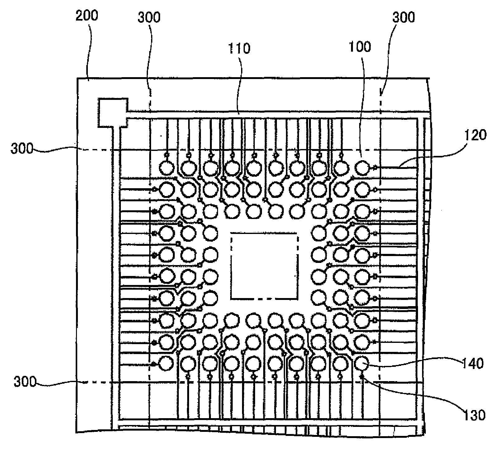
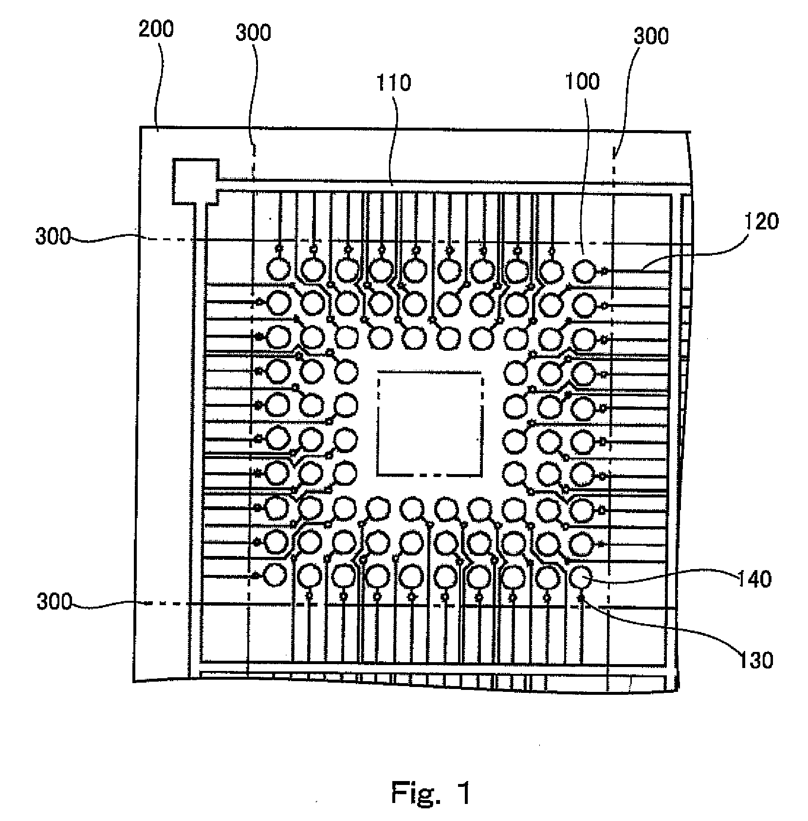
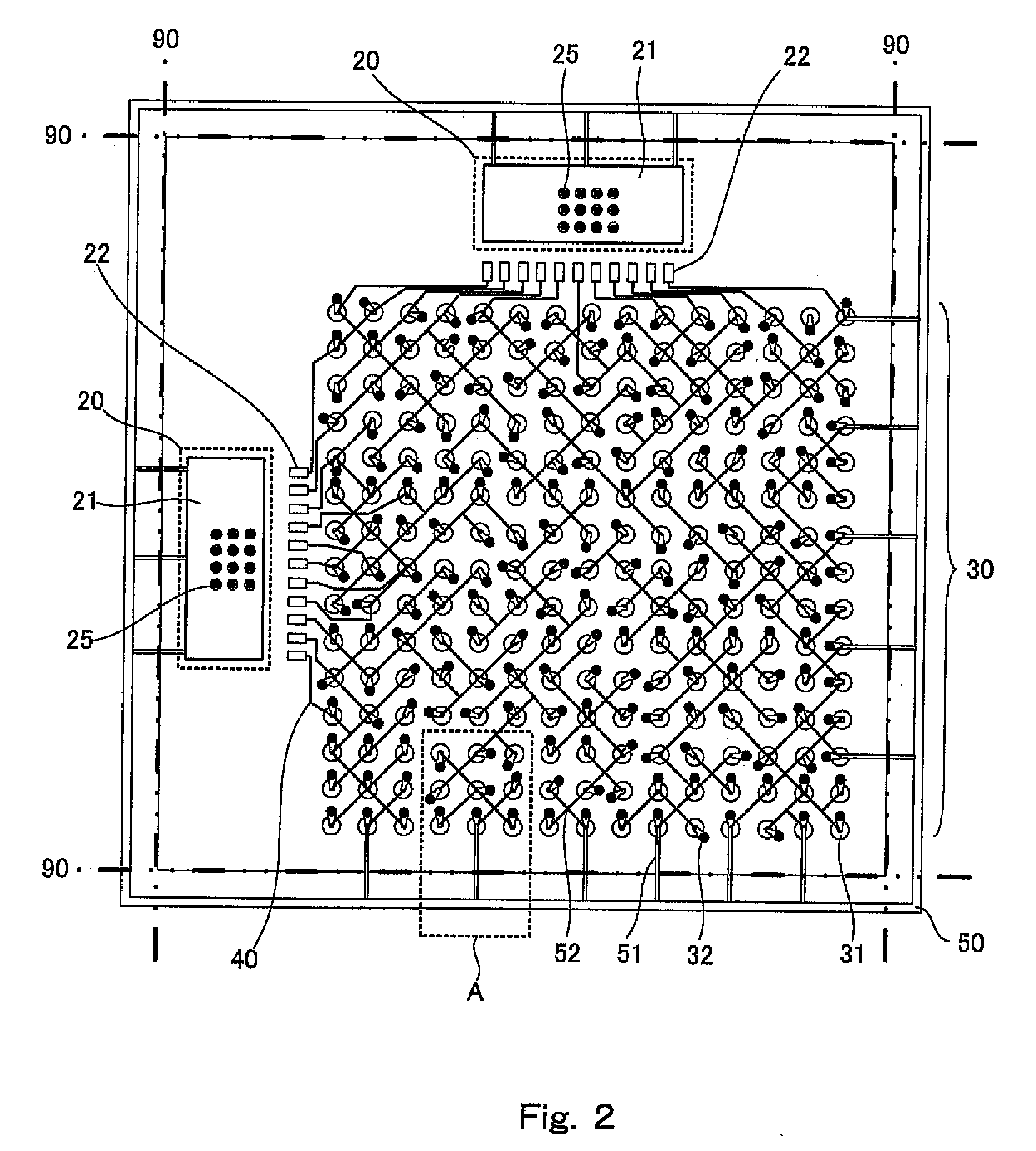
[0017]A preferred embodiment of the present invention is described below with reference to the attached drawings. FIG. 2 is a plan view showing the configuration of the obverse surface of the printed circuit board 10 according to an embodiment of the present invention. FIG. 3 is a plan view showing the configuration of the reverse surface according to an embodiment of the present invention. The drawings show a state prior to an Au plating process to be carried out on a variety of pads.

[0018]The printed circuit board 10 may be made of a glass epoxy resin, a paper phenolic resin, a paper epoxy resin, or the like. A chip mounting area 20 in which IC chips are to be mounted and a BGA mounting area 30 in which a BGA package is to be mounted are provided on the obverse surface of the printed circuit board 10. A die pad 21 is provided in the chip mounting area 20, and an IC chip is soldered or otherwise mounted on the die pad 21. The IC chips mounted on the printed circuit board 10 are con...


PUM

PropertyMeasurementUnit
electroconductiveaaaaaaaaaa
shapeaaaaaaaaaa
separation distanceaaaaaaaaaa

Abstract

There is provided a method for manufacturing a printed circuit board having an insulative board and a plurality of electroconductive pads arranged in a grid shape on the insulative board, the method comprising: a step for forming an electroconductive film on the insulative board; a step for forming a pattern on the electroconductive film so as to form the electroconductive pads, a lead wire connected to at least one of the electroconductive pads, and inter-pad wiring for electrically connecting each of the electroconductive pads not connected to the lead wire to any of the electroconductive pads connected to the lead wire, the inter-pad wiring being disposed between mutually adjacent electroconductive pads; a step for plating each of the electroconductive pads by immersing the insulative board in a plating bath and energizing each of the electroconductive pads through the lead wire; and a step for removing the inter-pad wiring.

Description

BACKGROUND OF THE INVENTION[0001]1. Technical field[0002]The present invention relates to a method for manufacturing a printed circuit board for mounting a semiconductor device and other electronic components.[0003]2. Description of the Related Art[0004]There are known in the art plastic packages in which ICs, LSIs, or other semiconductor chips are mounted on a printed circuit board, and a resin is injected into the chip mounting section to seal the package. A BGA (ball grid array) configuration is commonly used for such plastic packages in order to provide a larger number of terminals for the semiconductor chips to be mounted and to reduce the size of the package.[0005]A plurality of bonding pads, conductive wires, and the like are formed on the obverse surface of printed circuit boards used in BGA-type plastic packages, while a plurality of solder ball pads for forming solder balls as external connection terminals is formed in a grid shape on the reverse surface. Each of the solde...

Claims


Application Information

Patent Timeline
Patent Type & Authority Applications(United States)
IPC IPC(8): H05K3/00
CPCH05K1/111Y10T29/49162H05K3/06H05K3/242H05K3/42H05K2201/09254H05K2201/10719H05K2201/10734H05K2203/1572H05K2203/175H05K1/114Y10T29/49156H01L2224/48091H01L2224/48227H01L2924/15311H01L2924/00014
Inventor EGAWA, YOSHIMIKOBAYASHI, HARUFUMI
Owner LAPIS SEMICON CO LTD
Why Eureka
Try Eureka