Low cost substrates and method of forming such substrates

a technology of engineered substrates and substrates, applied in the direction of transportation and packaging, layered products, transistors, etc., can solve the problems of bonding defects observed when lower quality or excessively reclaimed materials are used for supports, and achieve the effect of low cost and lower quality

Active Publication Date: 2009-12-31
SOITEC SA
View PDF54 Cites 0 Cited by
  • Summary
  • Abstract
  • Description
  • Claims
  • Application Information

AI Technical Summary

Benefits of technology

[0016]Preferred manufacturing methods of the invention include providing a support having surface pits, depositing an intermediate layer of amorphous material on the pitted surface of the support so as to at least partially fill the pits, annealing the intermediate layer, assembling a donor wafer with the annealed intermediate support to form an intermediate structure, and reducing the thickness of the intermediate structure to form the final substrate.

Problems solved by technology

It is believed that bonding defects observed when lower quality or excessively reclaimed materials are used for supports originate from surface imperfections associated with crystalline defects in the support materials.

Method used


Image

  • Low cost substrates and method of forming such substrates
  • Low cost substrates and method of forming such substrates
  • Low cost substrates and method of forming such substrates

Examples


Embodiment Construction

[0023]This subsection describes, first, preferred embodiments of engineered substrates, and second, preferred embodiments of methods for their manufacture. The preferred embodiments and particular examples described herein should be seen as examples of the scope of the invention, but not as limiting the present invention. The scope of the present invention should be determined with reference to the claims.

[0024]Although most examples are directed to silicon substrates, the invention is not limited to silicon but can be used to manufacture engineered substrates of a wide variety of semiconductor or other materials or stacks thereof. Additionally, the invention can be used with supports or donor substrates in which devices have already been formed.

Support Substrate

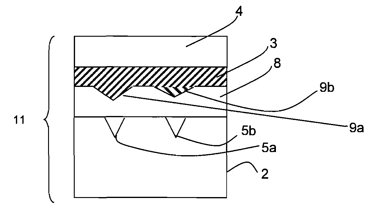
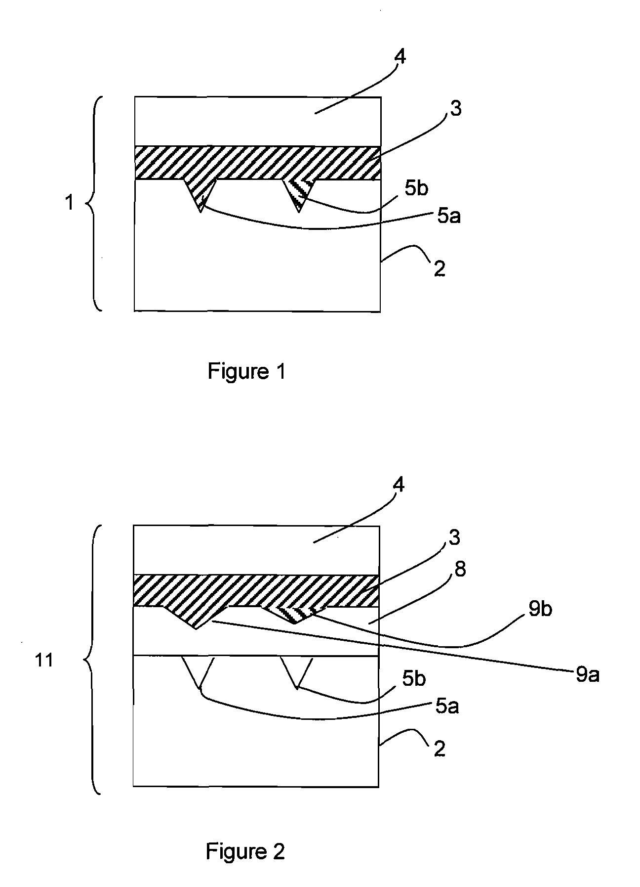
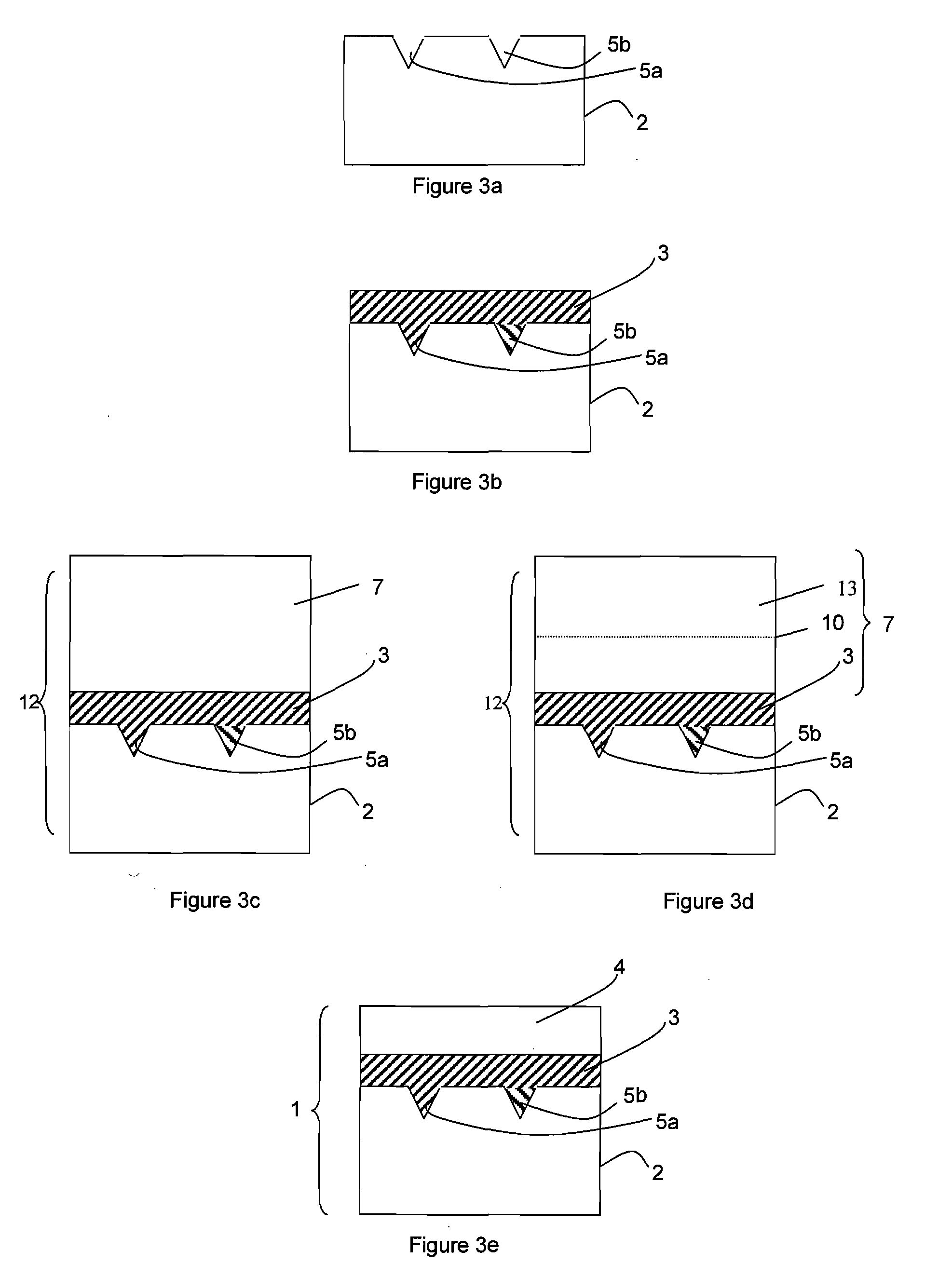
[0025]FIG. 1 illustrates a preferred embodiment of an engineered substrate of the invention. This illustrated substrate comprises support 2 with surface pits 5a and 5b having typical sizes between about 50 nm and 200 nm in ...


PUM


Abstract

In one embodiment, the invention provides engineered substrates having a support with surface pits, an intermediate layer of amorphous material arranged on the surface of the support so as to at least partially fill the surface pits, and a top layer arranged on the intermediate layer. The invention also provides methods for manufacturing the engineered substrates which deposit an intermediate layer on a pitted surface of a support so as to at least partially fill the surface pits, then anneal the intermediate layer, then assemble a donor substrate with the annealed intermediate layer to form an intermediate structure, and finally reduce the thickness of the donor substrate portion of the intermediate structure in order to form the engineered substrate.

Description

[0001]This application claims the benefit of U.S. application Ser. No. 61 / 093,877 filed Sep. 3, 2008, the entire content of which is expressly incorporated herein by reference thereto.BACKGROUND OF THE INVENTION[0002]The present invention relates to low cost, engineered substrates and their fabrication; such substrates find application in the fields of, e.g., microelectronics, optoelectronics, photovoltaics, micromechanics, high power microelectronics, and the like.BACKGROUND OF THE INVENTION[0003]Engineered substrates can be fabricated according to known techniques such as Smart Cut™ or bond and grind / etch back. Generally, a support is assembled with a donor substrate to form a temporary structure, the thickness of which is then reduced to form the final substrate. Thus, the final substrate often comprises a relatively thin top layer, the remaining thickness of thinned donor substrate, on a relatively thick support. An intermediate layer, e.g., an insulating layer, can be inserted ...

Claims


Application Information

Patent Timeline
Patent Type & Authority Applications(United States)
IPC IPC(8): H01L27/12H01L21/762
CPCH01L21/76254Y10T428/24851H01L21/76256
Inventor NGUYEN, BICH-YENMAZURE, CARLOS
Owner SOITEC SA
Why Eureka
Try Eureka