Adaptive Capacitive Sensing

a capacitive sensing and capacitive technology, applied in the direction of resistance/reactance/impedence, instruments, pulse techniques, etc., can solve the problems of capacitive sensors mistriggering or not functioning properly, touch pad false triggering, mobile devices configured with touch sensors especially present significant challenges, etc., to minimize in-band signal interference and minimize emi susceptibility

Inactive Publication Date: 2009-12-31
STANDRD MICROSYSTEMS CORPORATION
View PDF2 Cites 116 Cited by
  • Summary
  • Abstract
  • Description
  • Claims
  • Application Information

AI Technical Summary

Benefits of technology

[0011]A capacitive sensing circuit may comprise a resistive-capacitive bridge circuit with a signal path and a reference path, with the signal path configured to connect to the capacitance to be detected. A switching signal may simultaneously be applied to the signal path and the reference path, and a difference signal representative of a difference between the reference path signal and the signal path signal may be obtained. Small perturbations in the capacitance may be detected by mixing / correlating the difference signal to the switching signal. It should be noted that as described herein, correlation is performed by mixing two signals, where the output generated by the mixing operation is indicative of the level of correlation between the two signals. The output of the mixer / correlator may be filtered using narrowband low-pass filters to virtually eliminate all EMI signals. Since the narrowband approach allows filtering out unwanted signals, it enables operation in systems that are susceptible to high levels of noise. The bridge circuit may also provide low impedance at the button node to minimize EMI susceptibility. Frequency stepping the switching signal with specified frequency increments may minimize in-band signal interference, and allow operation in the presence of many signals that would otherwise result in failure of the sensing circuit. Pad calibration may also be implemented to free the user from a need to characterize each button channel capacitance and tailor the operation for each channel.

Problems solved by technology

Mobile devices configured with touch sensors especially present significant challenges, due to highly variable environmental conditions to which they may be subjected.
Electrostatic discharge is another potential cause for capacitive sensors mistriggering or not functioning properly, and water and other contaminants can cause similar problems.
However, one weakness of today's products remains their susceptibility of the sensor to coupling unwanted large electromagnetic signals onto the [touch] pad, which typically corrupts the sensor output such that false touches are reported, or, in other words, resulting in false triggering of the touch pad.
Most of these solutions, however, have difficulty insuring proper operation in the presence of a high EMI environment, and false detections have caused problems in many PC applications.

Method used


Image

  • Adaptive Capacitive Sensing
  • Adaptive Capacitive Sensing
  • Adaptive Capacitive Sensing

Examples


Embodiment Construction

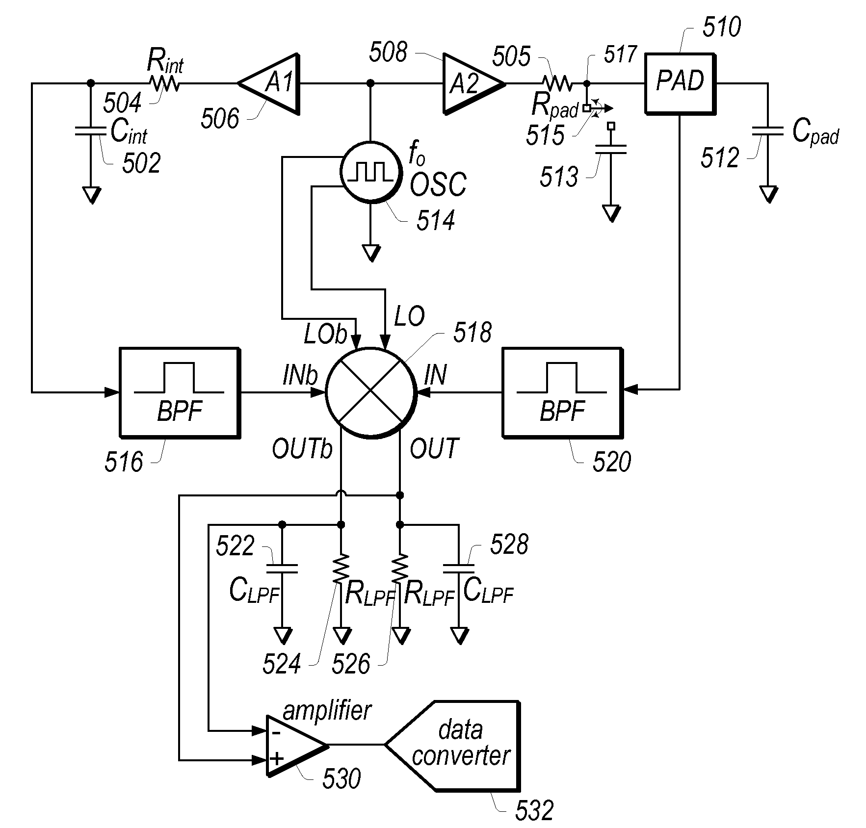
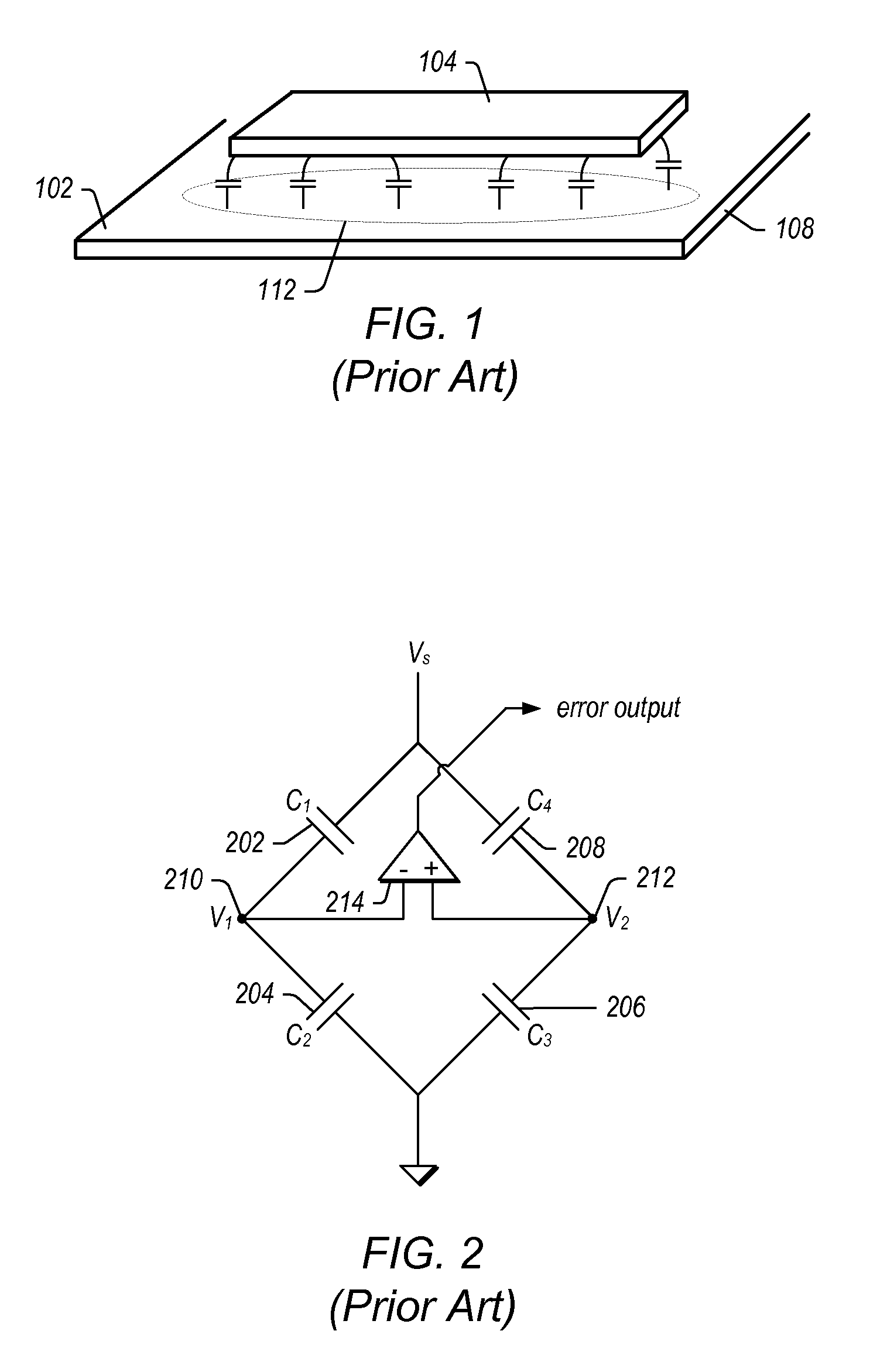
[0031]Various embodiments of the present invention comprise a capacitive sensing system capable of detecting an increase in capacitance on a pad that may occur when an object, such as a fingertip is near the pad or touches the pad. It should be noted that in many embodiments, the actual surface of the pad may be covered with an insulating layer, in which case the insulating layer may be considered a part of the pad, and touching the pad may be interpreted as touching the insulating layer. As shown in FIG. 1, a metal pad 104 may be configured on circuit board 102 comprising a ground layer 108. The capacitance between metal pad 104 and the ground layer 108 is illustrated by capacitance 112.l Placing an object, such as a human finger near or on pad 104 may result in added capacitance between pad 104 and ground, thereby increasing the pad capacitance. Typical parasitic pad capacitance (i.e. capacitance 112) may range from 5 pF to 50 pF, while typical capacitance increase from a human fi...


PUM


Abstract

A capacitive sensing circuit may comprise an RC (resistive-capacitive) bridge circuit, with a switching signal simultaneously applied to a reference path, and a signal path comprising the capacitance to be detected. Small perturbations in the capacitance may be detected by mixing / correlating a difference signal representative of the difference between the reference path signal and the signal path signal, to the switching signal. The output of the mixer may be filtered to virtually eliminate all EMI signals. A narrowband approach may also allow filtering of unwanted signals, enabling operation in systems susceptible to high levels of noise. Frequency stepping of the switching signal may minimize inband signal interference, and allow operation in the presence of many signals that would otherwise result in failure of the sensing circuit. Pad calibration may be implemented to free the user from a need to characterize each button channel capacitance and tailor the operation for each channel.

Description

PRIORITY CLAIM[0001]This application is a continuation-in-part of U.S. Provisional Application Ser. No. 61 / 076,482 titled “Adaptive Capacitive Sensing” filed Jun. 27, 2008, whose inventor was Scott C. McLeod, and which is hereby incorporated by reference in its entirety as though fully and completely set forth herein.BACKGROUND OF THE INVENTION[0002]1. Field of the Invention[0003]This invention relates generally to the field of semiconductor circuit design, and more particularly to the design of an adaptive capacitive sensing circuit.[0004]2. Description of the Related Art[0005]It's been a high priority for many electronics manufacturers to offer user interfaces that are powerful yet simple to use, while remaining highly reliable. Some of the more popular interfaces have been touchscreens and touchpads. Touchscreens and touchpads can typically detect the location of touches within the display / pad area, allowing the display / pad to be used as an input device, and in the case of touchs...

Claims


Application Information

Patent Timeline
Patent Type & Authority Applications(United States)
IPC IPC(8): G01R27/26G06F15/00G06F3/045
CPCG06F3/0416G06F3/044H03K2217/96075H03K17/962H03K17/002
Inventor MCLEOD, SCOTT C.
Owner STANDRD MICROSYSTEMS CORPORATION
Why Eureka
Try Eureka