Supercharge Your Innovation With Domain-Expert AI Agents!

Circuit with one or more depletion mode transistors

a transistor and depletion mode technology, applied in pulse generators, instruments, pulse techniques, etc., can solve the problems of limiting high frequency performance, h-bridge topology when used as a power amplifier in high frequency radio applications can have limitations, and modulation formats with large peak-to-average ratios typically exhibit poor efficiency when amplified by tuned amplifier topologies

Inactive Publication Date: 2010-01-07
GOOGLE TECH HLDG LLC
View PDF15 Cites 11 Cited by
  • Summary
  • Abstract
  • Description
  • Claims
  • Application Information

AI Technical Summary

Problems solved by technology

As a result, modulation formats which have large peak-to-average ratios typically exhibit poor efficiency when amplified by tuned amplifier topologies.
The H-Bridge topology when used as a power amplifier in high frequency radio applications can have limitations when using both P-channel enhancement-mode Field Effect Transistors (FETs) and N-channel enhancement-mode FETs.
The larger device increases shunt capacitance, further limiting high frequency performance.
However, such a configuration presents a challenging driver design problem as the source voltage of the upper transistors are not fixed.
Thus, although the all N-channel H-Bridge topologies are able to operate at high frequencies as power amplifiers, they require relatively large gate voltage swings to control (switch) the upper transistors.

Method used


Image

  • Circuit with one or more depletion mode transistors
  • Circuit with one or more depletion mode transistors
  • Circuit with one or more depletion mode transistors

Examples


Embodiment Construction

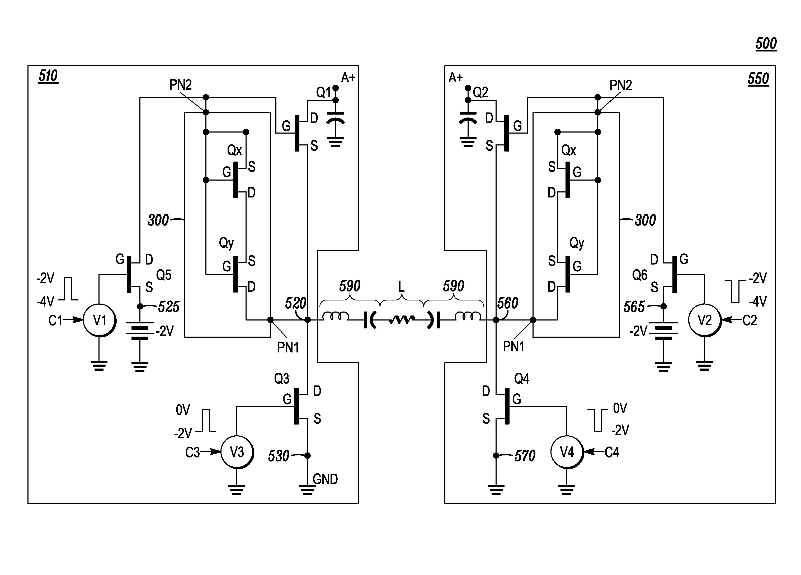
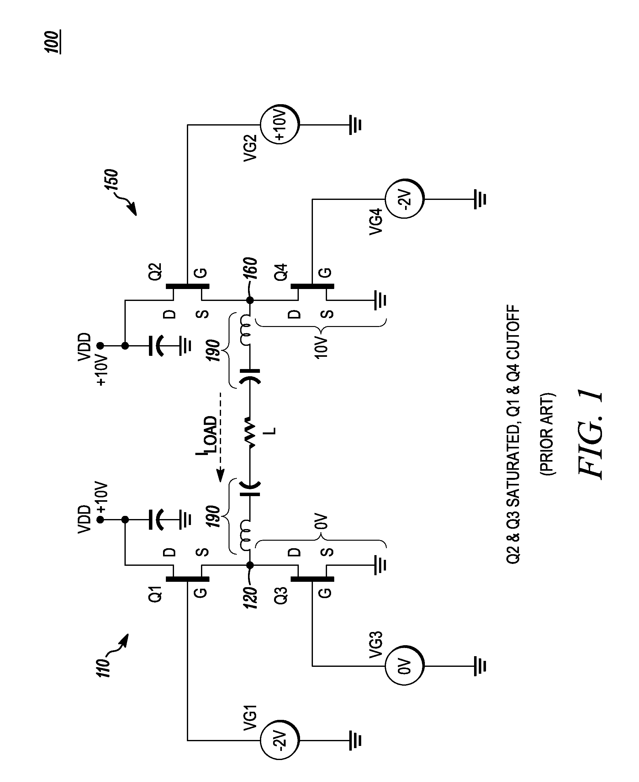
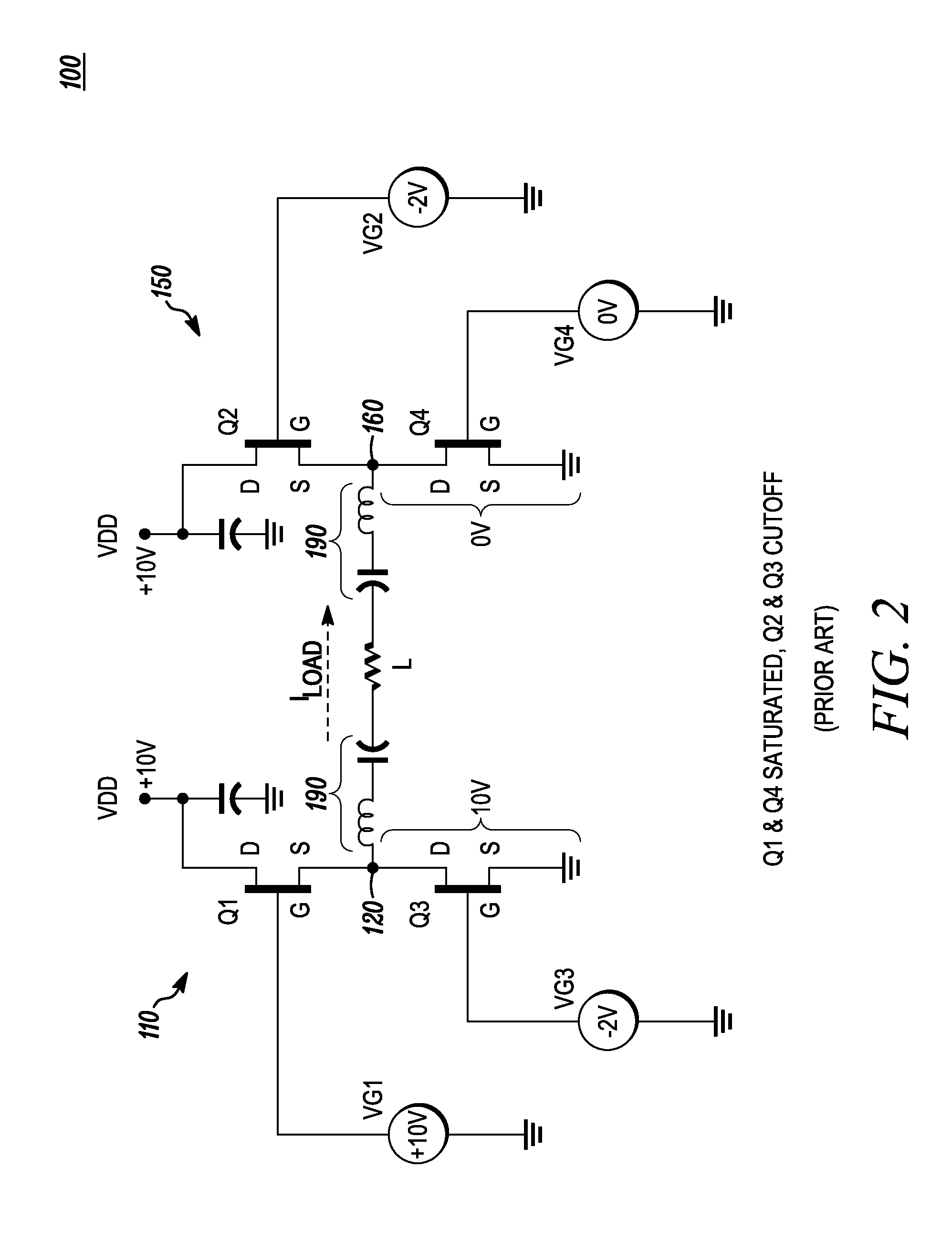
[0019]Before describing in detail embodiments that are in accordance with the present invention, it should be observed that the embodiments reside primarily in circuit components. Accordingly, the circuit components have been represented where appropriate by conventional symbols in the drawings, showing only those specific details that are pertinent to understanding the embodiments of the present invention so as not to obscure the disclosure with details that will be readily apparent to those of ordinary skill in the art having the benefit of the description herein.

[0020]In this document, relational terms such as first and second, top and bottom, and the like may be used solely to distinguish one entity or action from another entity or action without necessarily requiring or implying any actual such relationship or order between such entities or actions. The terms “comprises,”“comprising,” or any other variation thereof, are intended to cover a non-exclusive inclusion, such that dev...


PUM


Abstract

An H-bridge circuit formed from two sub-circuits coupled to each other by a load network across a respective load node of each of the sub-circuits. Each sub-circuit of the two sub-circuits comprises a depletion mode upper transistor with a second electrode coupled to a first electrode of a lower transistor. The load node of the sub-circuit is disposed between the second electrode of the upper transistor and the first electrode of a lower transistor. There is a first voltage supply node coupled to a first electrode of the upper transistor and a second voltage supply node is coupled to a second electrode of the lower transistor. An upper driver transistor selectively couples a gate electrode of the upper transistor to an upper drive voltage node, the upper driver transistor having a control electrode coupled to an upper switched voltage supply circuit. There is also a lower switched voltage supply circuit coupled to a gate electrode of the lower transistor and a voltage dependent non-linear resistor is coupled across the gate electrode and second electrode of the upper transistor. In use, when the lower transistor and upper driver transistor are in a non-conductive state a potential difference across the voltage dependent non-linear resistor is sufficiently small enough to control the upper transistor into a conductive state. Conversely, when the lower transistor and upper driver transistor are in a conductive state the potential difference across the voltage dependent non-linear resistor provides a negative bias to the gate electrode of the upper transistor that has a negative potential sufficient to control the upper transistor into a non-conductive state.

Description

FIELD OF THE INVENTION[0001]The present invention relates generally to circuits comprising one or more depletion mode transistors. The invention is specifically useful for, but not necessarily limited to, H-Bridge or half H-Bridge circuits used for conversion of digital data to high power Radio Frequency signals or radio frequency power amplification.BACKGROUND OF THE INVENTION[0002]Circuits that include transistors used as controllable switches or variable resistors come in various topologies including H-Bridge topologies, half H-bridge topologies and tuned amplifier topologies. Further, circuits operating as Radio Frequency (RF) power amplifiers have traditionally been implemented in a tuned amplifier topology in which input and output networks of the power amplifiers effectively resonate at a desired operating frequency. Resonant frequency operation allows parasitic reactance, such a shunt capacitance and series inductance, to be absorbed into the networks, thereby maximizing the...

Claims


Application Information

Patent Timeline
Patent Type & Authority Applications(United States)
IPC IPC(8): G05F1/00
CPCH03F3/2173
Inventor CYGAN, LAWRENCE F.KHAN, ANDREW M.WILLIAMS, CURTIS M.
Owner GOOGLE TECH HLDG LLC
Features
  • R&D
  • Intellectual Property
  • Life Sciences
  • Materials
  • Tech Scout
  • Unparalleled Data Quality
  • Higher Quality Content
  • 60% Fewer Hallucinations
Learn More