Semiconductor integrated circuit

a technology of integrated circuits and semiconductors, applied in the direction of semiconductor devices, electrical equipment, transistors, etc., can solve the problems of increasing an area and performance degradation of semiconductor integrated circuits, affecting transistor characteristics, and affecting the characteristics of transistors, so as to suppress the variation in the characteristics of basic logic cells, suppress the overhead of chip area, and suppress the effect of transistor characteristics

Inactive Publication Date: 2010-01-14
RENESAS ELECTRONICS CORP
View PDF25 Cites 64 Cited by
  • Summary
  • Abstract
  • Description
  • Claims
  • Application Information

AI Technical Summary

Benefits of technology

[0024]According to the present invention, it is possible to suppress variation in characteristics of the basic logic cell that depend on the surrounding layout pattern. Moreover, since it is not necessary to place the dummy cells in a gate array form to surround the basic logic cell, the overhead of the chip area can be suppressed.
[0025]Furthermore, it is possible to suppress the variation in the transistor characteristics caused by the peripheral layout pattern, without modifying the arrangement of basic logic cells and the cell library of the basic logic cells. Moreover, it is possible to suppress variation in the gate size and the STI stress at the time of manufacturing.

Problems solved by technology

However, if regions having different local pattern densities exist on the wafer surface as in the cell-based IC, the wafer surface may not become planar and thus a film thickness of the polished film may not become uniform even after the polishing.
However, the above-mentioned techniques for suppressing the variation of the transistor characteristics may cause increase in an area and performance degradation of the semiconductor integrated circuit.
Moreover, in recent years, a ratio of variation in an interconnection width due to the OPE (Optical Proximity Effect) to the original interconnection width is getting larger, which affects the transistor characteristics.
In the case where the dummy cell has not only the well but also the dummy patterns of diffusion layers and polysilicon for equalizing the local pattern density, the peripheral pattern surrounding the basic logic cell becomes complicated.
As the peripheral pattern becomes more complicated, the OPC procedure becomes more difficult, which causes increase in TAT (Turn Around Time).
However, it is difficult to make a distance (inter-diffusion-layer distance 120) between adjacent diffusion layers of the different basic logic cells 102 constant.
However, it is difficult to apply to a region where a large number of basic logic cells are placed.
Even if it is applied, an area becomes extremely large due to the gate array form.
Therefore, the gate or the diffusion layer may be short-circuited with another region due to malfunction of the dummy cell transistor, fine grains such as dust, and the like, which causes a problem.

Method used


Image

  • Semiconductor integrated circuit
  • Semiconductor integrated circuit
  • Semiconductor integrated circuit

Examples


first embodiment

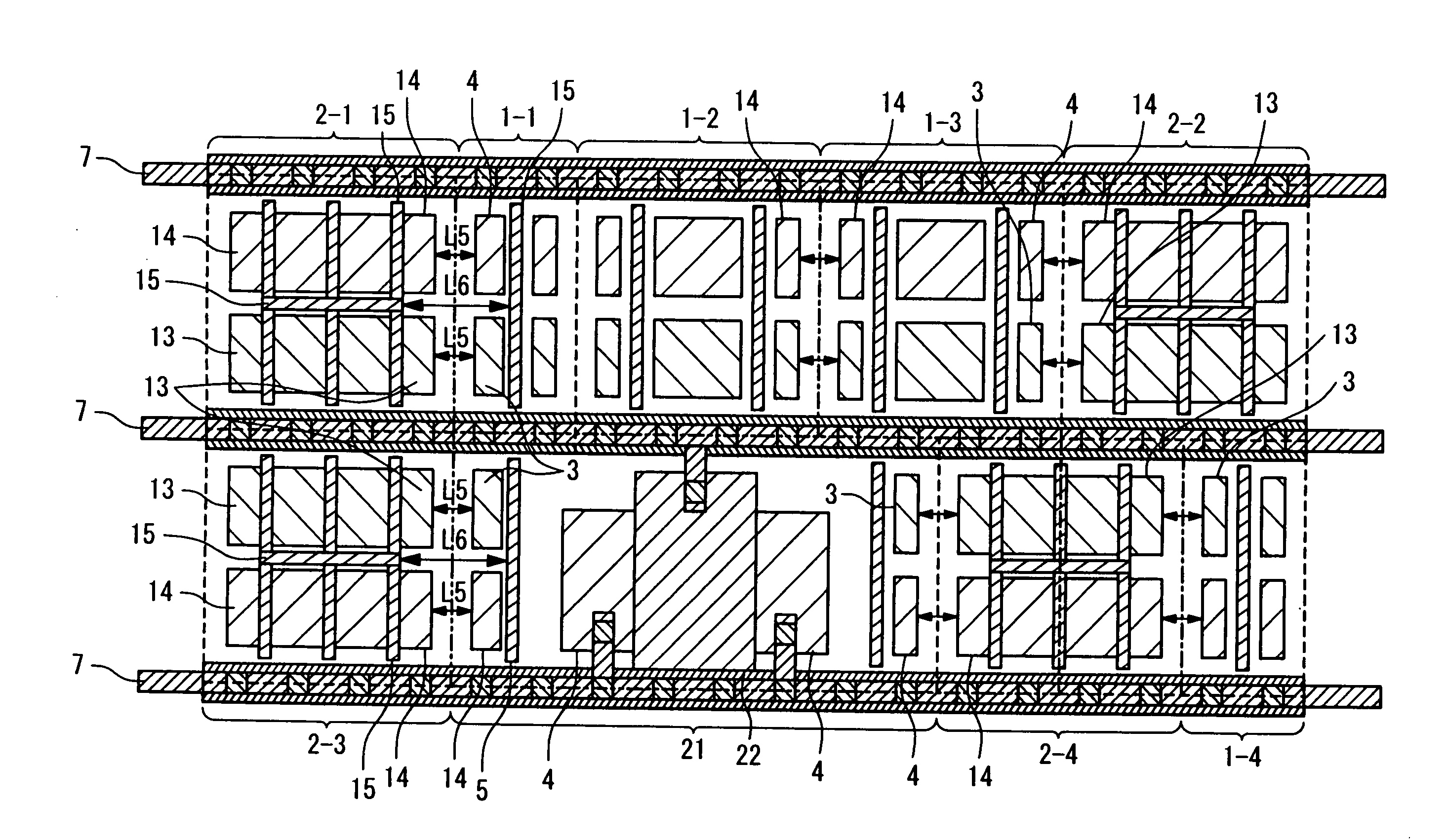
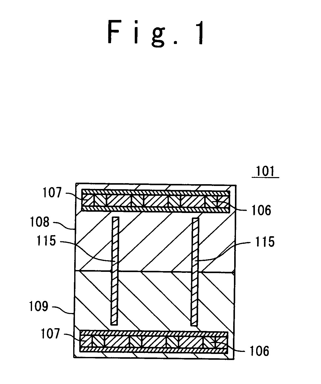
[0039]FIG. 3 is a plan view showing a configuration of a dummy cell 1 according to a first embodiment of the present invention. The dummy cell 1 includes a N well 8 and a P well 9. The N well 8 and the P well 9 are provided between two metal power-supply interconnections 7 connected to contacts 6. The dummy cell 1 further includes a dummy P+ diffusion layer 4 formed in the N well 8 and a dummy N+ diffusion layer 3 formed in the P well 9. The dummy cell 1 further includes a dummy gate polysilicon (dummy gate electrode) 5. The dummy gate polysilicon 5 is formed above the N well 8 and the P well 9. The dummy P+ diffusion layer 4 and the dummy gate polysilicon 5 of the dummy cell 1 are placed so as not to function as a transistor. Similarly, the dummy N+ diffusion layer 3 and the dummy gate polysilicon 5 of the dummy cell 1 are placed so as not to function as a transistor. In other words, the dummy diffusion layer (3, 4) is separated from the dummy gate polysilicon 5, when the dummy gat...

second embodiment

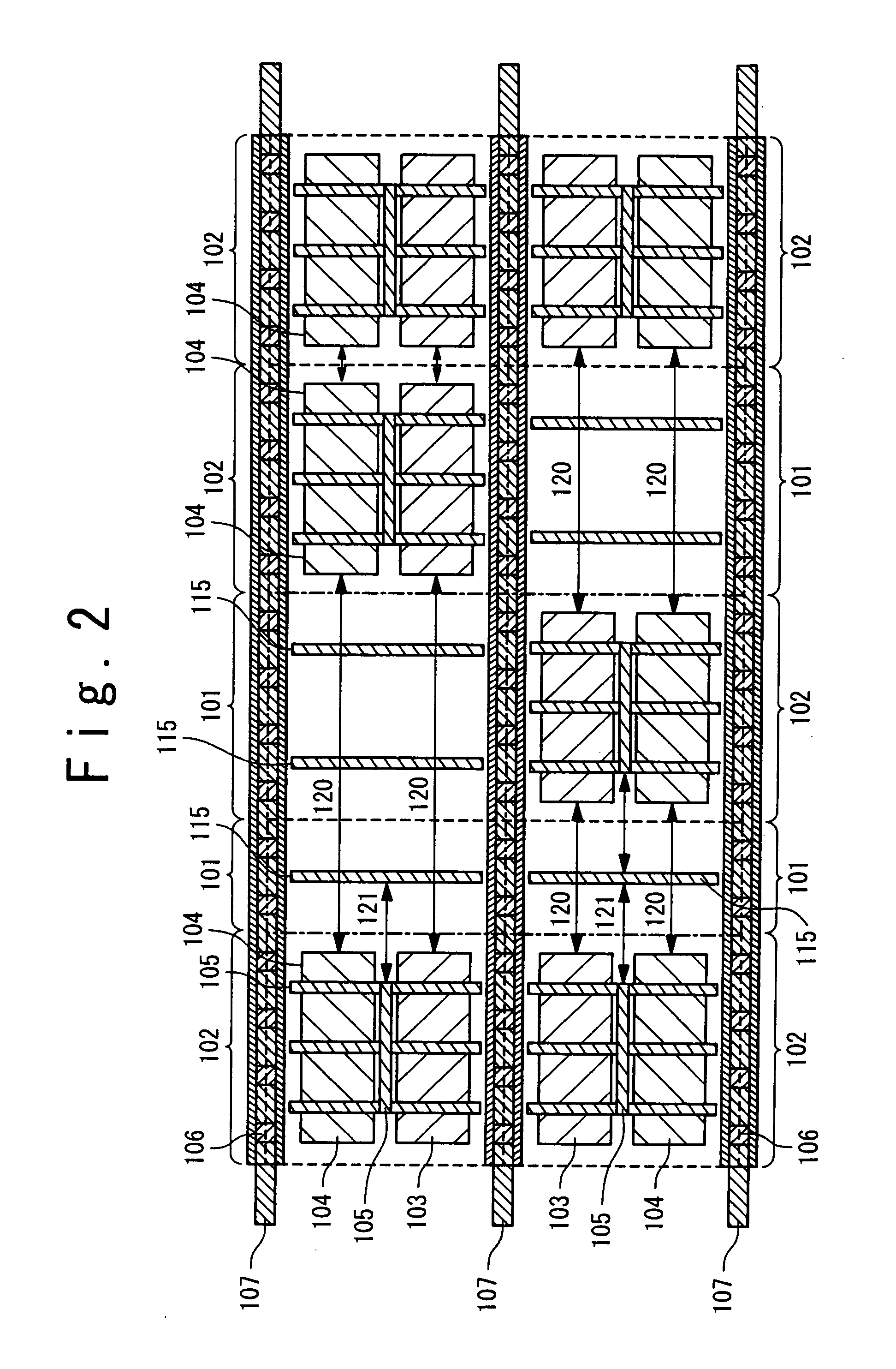
[0056]FIG. 6 is a plan view showing a configuration of a dummy cell 1 according to a second embodiment of the present invention. In general, several kinds of sizes are prepared for the dummy cell 1. In a case of a large-size dummy cell 1, it is preferable to uniformly provide dummy gate polysilicons 5 and diffusion layers within the cell in addition to the outermost dummy gate polysilicon 5 and the outermost diffusion layer, for the purpose of data uniformity and manufacturability.

[0057]As shown in FIG. 6, the dummy cell 1 in the second embodiment is provided with four dummy gate polysilicons 5 and the outermost diffusion layers (dummy N+ diffusion layers 3, dummy P+ diffusion layers 4). The dummy cell 1 in the second embodiment is further provided with one extra dummy N+ diffusion layer 3 and one extra dummy P+ diffusion layer 4 that are sandwiched between the inner two dummy gate polysilicons 5.

[0058]According to the dummy cell 1 of the second embodiment, the distance relationship...

third embodiment

[0059]FIG. 7 is a plan view showing a configuration of a dummy cell 1according to a third embodiment of the present invention. As shown in FIG. 7, the dummy cell 1 in the third embodiment is provided with seven dummy gate polysilicons 5 and the outermost diffusion layers (dummy N+ diffusion layers 3, dummy P+ diffusion layers 4). The dummy cell 1 in the third embodiment is further provided with extra dummy N+ diffusion layers 3 and extra dummy P+ diffusion layers 4 that are located between the inner three dummy gate polysilicons 5.

[0060]According to the dummy cell 1 of the third embodiment, the distance relationship is the same as in the first embodiment and the second embodiment. That is, the outermost dummy P+ diffusion layer 4 formed in the N well 8 has a side closest to an edge of the dummy cell 1, and a distance from the closest side to the edge of the dummy cell 1 is equal to the first distance L1. Similarly, the outermost dummy N+ diffusion layer 3 formed in the P well 9 has ...


PUM


Abstract

A semiconductor integrated circuit has: a substrate; a basic logic cell placed on the substrate and configured to function as a part of a logic circuit; and a dummy cell placed on the substrate and not configured to function as a part of a logic circuit. The basic logic cell includes a diffusion layer formed in the substrate, and a distance from the diffusion layer to a boundary between the basic logic cell and another cell adjacent to the basic logic cell is equal to a first distance. The dummy cell includes a dummy diffusion layer that is a diffusion layer formed in the substrate, and a distance from the dummy diffusion layer to a boundary between the dummy cell and another cell adjacent to the dummy cell is equal to the first distance.

Description

INCORPORATION BY REFERENCE [0001]This application is based upon and claims the benefit of priority from Japanese patent application No. 2008-182689, filed on Jul. 14, 2008, the disclosure of which is incorporated herein in its entirety by reference.BACKGROUND OF THE INVENTION [0002]1. Field of the Invention[0003]The present invention relates to a semiconductor integrated circuit.[0004]2. Description of Related Art[0005]Semiconductor integrated circuits (LSIs) called “semi-custom ICs” such as gate arrays and cell-based ICs (standard cells) have become popular. In the case of the cell-based IC, a desired circuit is achieved by placing basic logic cells such as a two-input NAND, an inverter and a flip-flop on a well (substrate). In the cell-based IC, regions where basic logic cells are placed and regions where no basic logic cell is placed are mixed.[0006]A process for fabricating a semiconductor integrated circuit includes CMP (Chemical Mechanical Polishing). In the CMP, a wafer surfa...

Claims


Application Information

Patent Timeline
Patent Type & Authority Applications(United States)
IPC IPC(8): H01L29/00
CPCH01L27/11803H01L27/0207
Inventor UEMURA, TOSHIFUMI
Owner RENESAS ELECTRONICS CORP
Why Eureka
Try Eureka