Recessed Germanium (Ge) Diode

a germanium diode and recessed technology, applied in the field of optoelectronic semiconductor fabrication, to achieve the effect of reducing the height of the ridge on the grown second material

Inactive Publication Date: 2010-01-14
ANALOG DEVICES INC
View PDF5 Cites 65 Cited by
  • Summary
  • Abstract
  • Description
  • Claims
  • Application Information

AI Technical Summary

Benefits of technology

[0009]The height of a ridge on the grown second material may be reduced, such as by heating the substrate, such as to a temperature between about 750° C. and about 900° C. Optionall

Problems solved by technology

However, growing Ge on a Si surface creates large steps, which pose problems for subsequent fi

Method used


Image

  • Recessed Germanium (Ge) Diode
  • Recessed Germanium (Ge) Diode
  • Recessed Germanium (Ge) Diode

Examples


Embodiment Construction

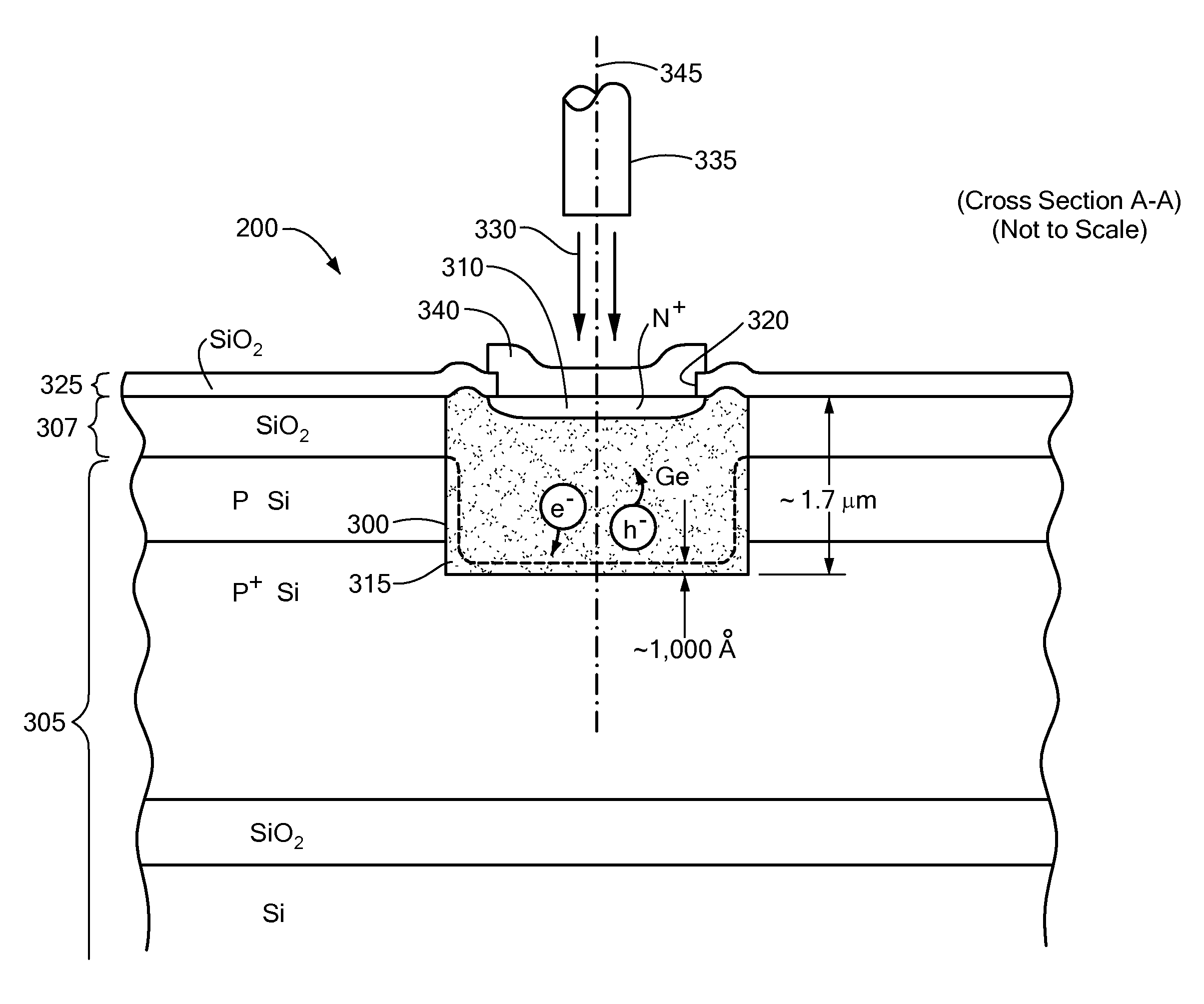
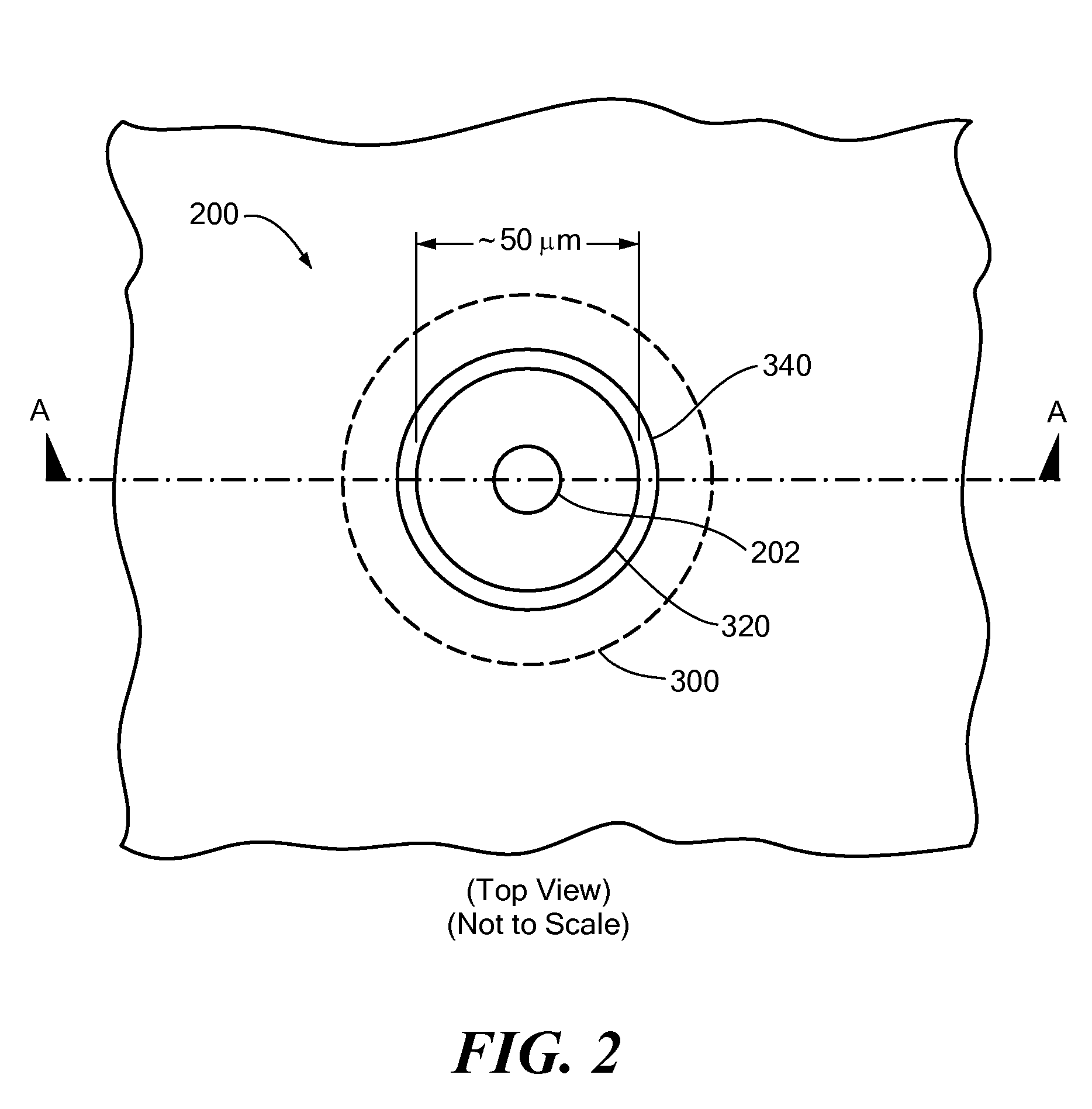
[0030]In accordance with the present invention, methods and apparatus are disclosed for providing a recessed germanium (Ge) region in a silicon (Si) substrate. The top of such a Ge region may be flush, or nearly flush, with the surrounding Si substrate or a passivation layer on the substrate, to facilitate subsequent semiconductor processing. However, the Ge region may be thick enough to obtain good coupling efficiencies to vertical, free-space light entering the Ge region. The Ge region may be fabricated by etching a hole through the passivation layer and into the Si substrate and then growing Ge in the hole by a selective epitaxial process.

BACKGROUND

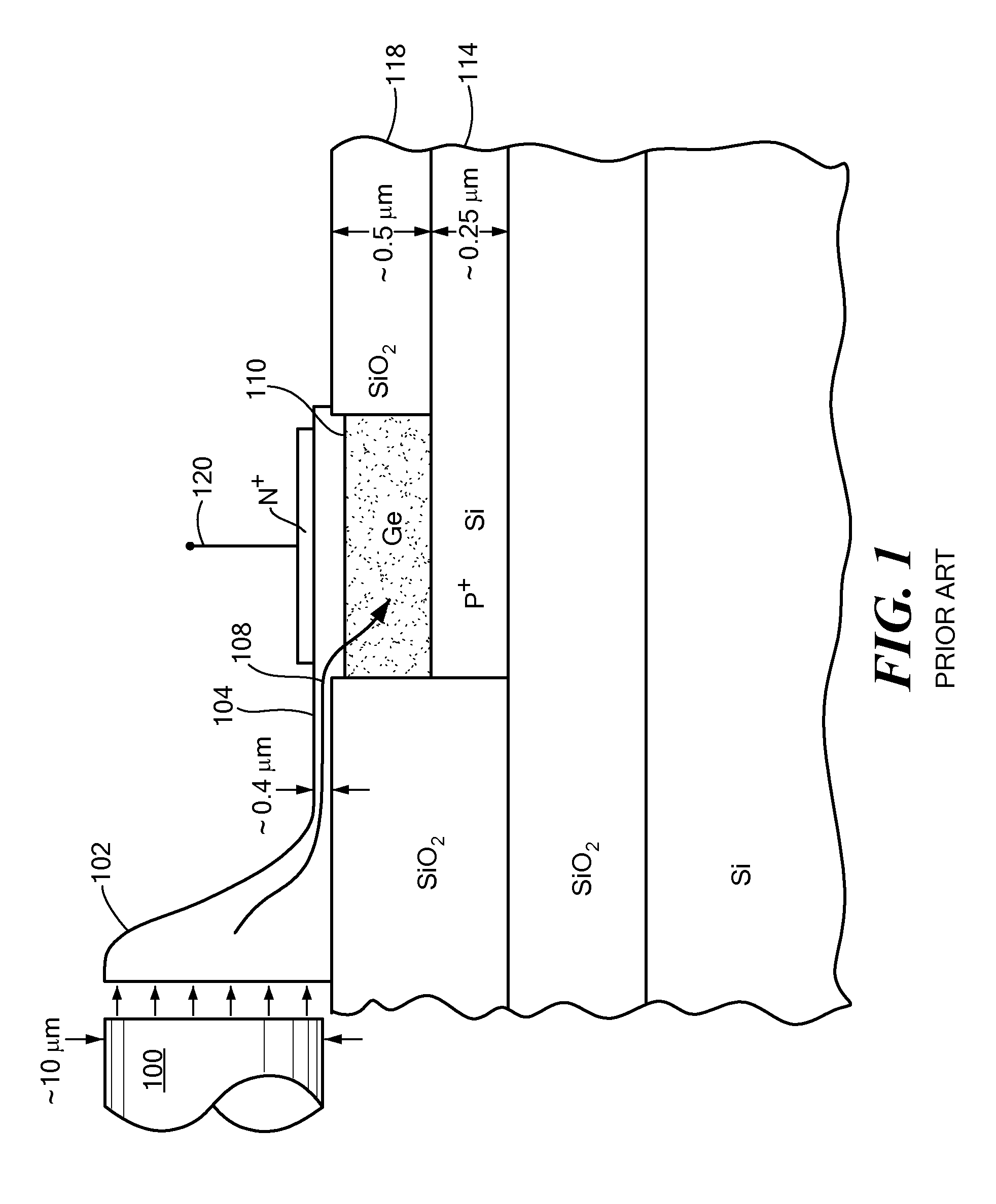
[0031]High-speed optical communication systems typically include optical fibers to carry optical signals and photodetectors coupled to the ends of the optical fibers to detect the optical signals and to convert the optical signals into electrical signals. Group 3-5 compound semiconductor photodiodes are commonly used as the photodetect...


PUM


Abstract

A photodiode is formed in a recessed germanium (Ge) region in a silicon (Si) substrate. The Ge region may be fabricated by etching a hole through a passivation layer on the Si substrate and into the Si substrate and then growing Ge in the hole by a selective epitaxial process. The Ge appears to grow better selectively in the hole than on a Si or oxide surface. The Ge may grow up some or all of the passivation sidewall of the hole to conformally fill the hole and produce a recessed Ge region that is approximately flush with the surface of the substrate, without characteristic slanted sides of a mesa. The hole may be etched deep enough so the photodiode is thick enough to obtain good coupling efficiencies to vertical, free-space light entering the photodiode.

Description

TECHNICAL FIELD[0001]The present invention relates to optoelectronic semiconductor fabrication and, more particularly, to fabrication of a recessed germanium (Ge) diode in a silicon substrate.BACKGROUND ART[0002]Demand for low cost and high density near infrared (NIR) solid-state detectors has motivated development and use of germanium on silicon (Ge / Si) heterostructures to extend the optoelectronic application of Si technology. Ge / Si structures are currently being considered for NIR P / N detectors that can be integrated with Si complementary metal-oxide-semiconductor (CMOS) devices. Various research demonstrations of integrated Ge / Si diodes with CMOS have been made, including using sputtered polycrystalline germanium (poly-Ge) to form Ge / Si photodiodes after CMOS transistors were complete. Poly-Ge may be formed by various methods, including the use of plasma enhanced chemical vapor deposition (PECVD).[0003]When integrating Ge on a Si substrate, such as for use as a free-space couple...

Claims


Application Information

Patent Timeline
IPC IPC(8): H01L31/00H01L21/00
CPCH01L27/1443H01L31/18H01L31/074
Inventor YASAITIS, JOHN A.LOWELL, LAWRENCE JAY
Owner ANALOG DEVICES INC
Why Eureka
Try Eureka