

Storage nitride encapsulation for non-planar sonos NAND flash charge retention
a technology of storage nitride and charge retention, which is applied in the direction of semiconductor devices, semiconductor/solid-state device details, electrical apparatus, etc., can solve problems such as retention concerns
- Summary
- Abstract
- Description
- Claims
- Application Information
AI Technical Summary
Benefits of technology
Problems solved by technology
Method used
Image

Examples
Embodiment Construction
[0004]It is to be understood that the following disclosure provides many different embodiments, or examples, for implementing different features of various embodiments. Specific examples of components and arrangements are described below to simplify the present disclosure. These are, of course, merely examples and are not intended to be limiting. In addition, the present disclosure may repeat reference numerals and / or letters in the various examples. This repetition is for the purpose of simplicity and clarity and does not in itself dictate a relationship between the various embodiments and / or configurations discussed.
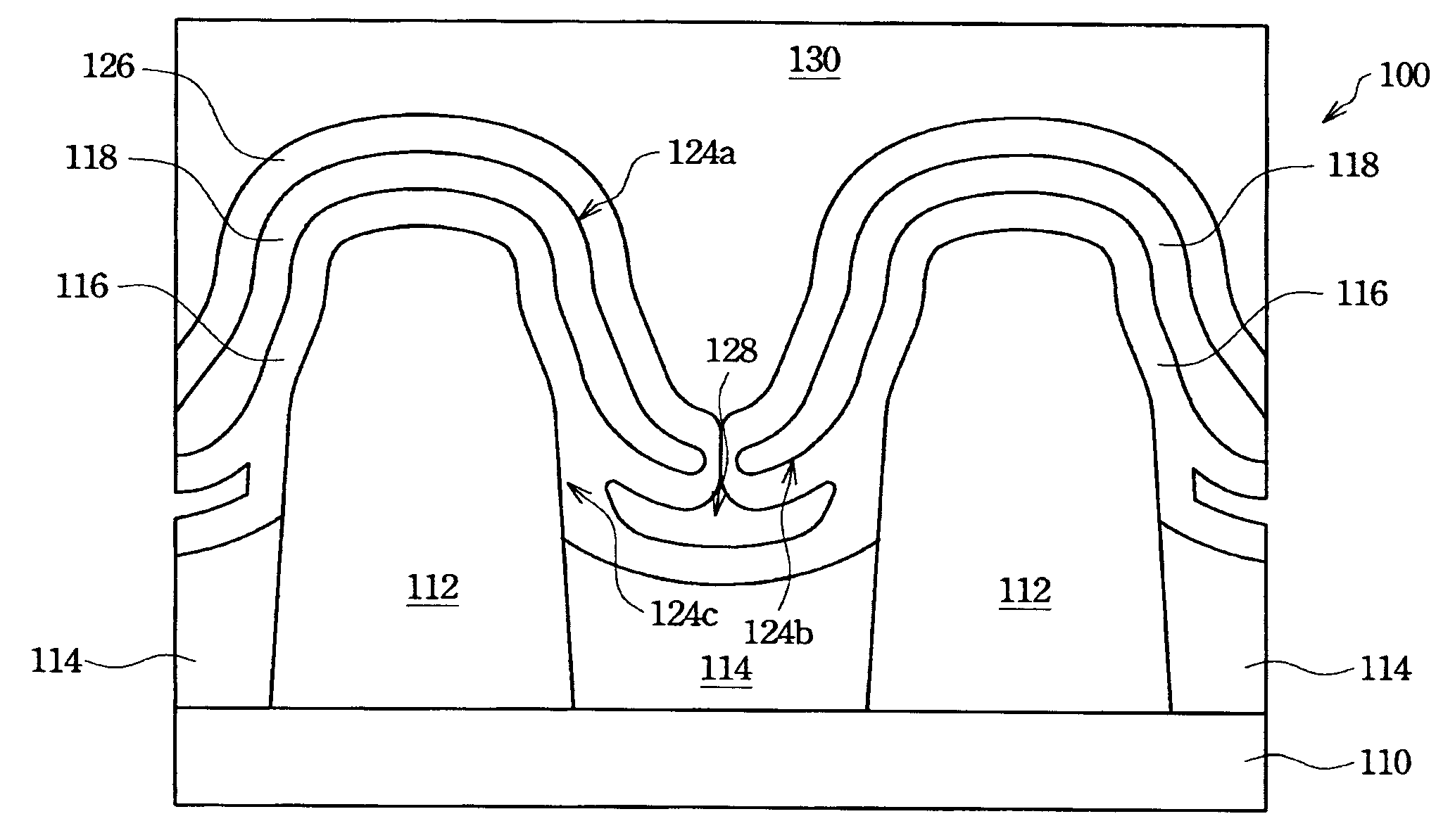
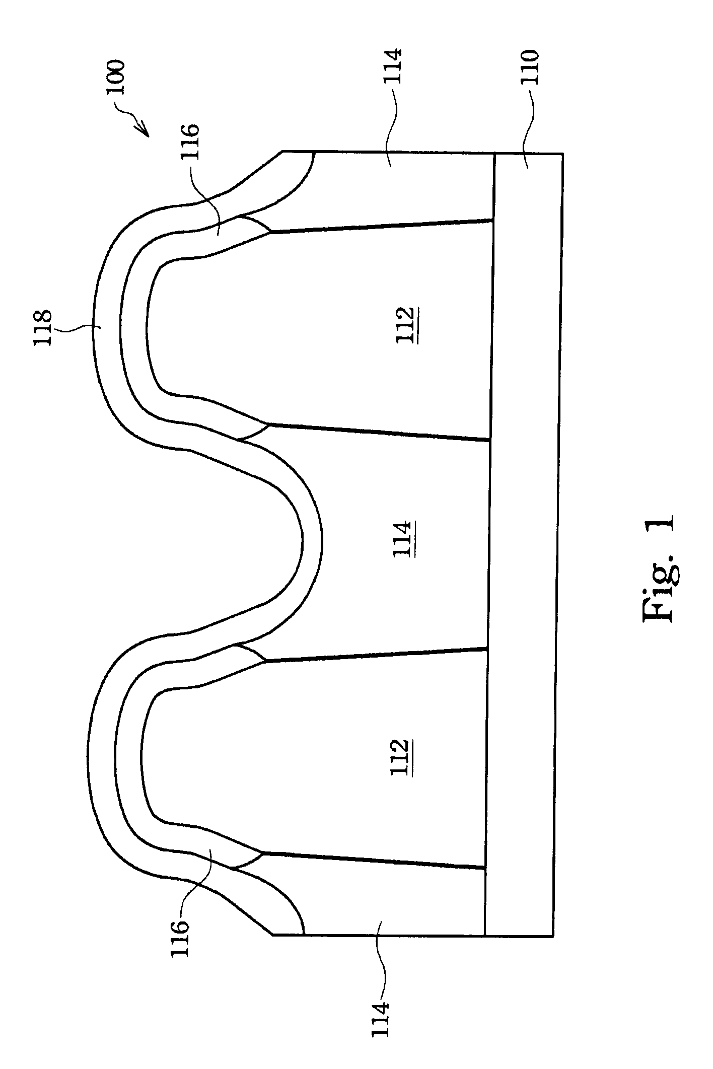
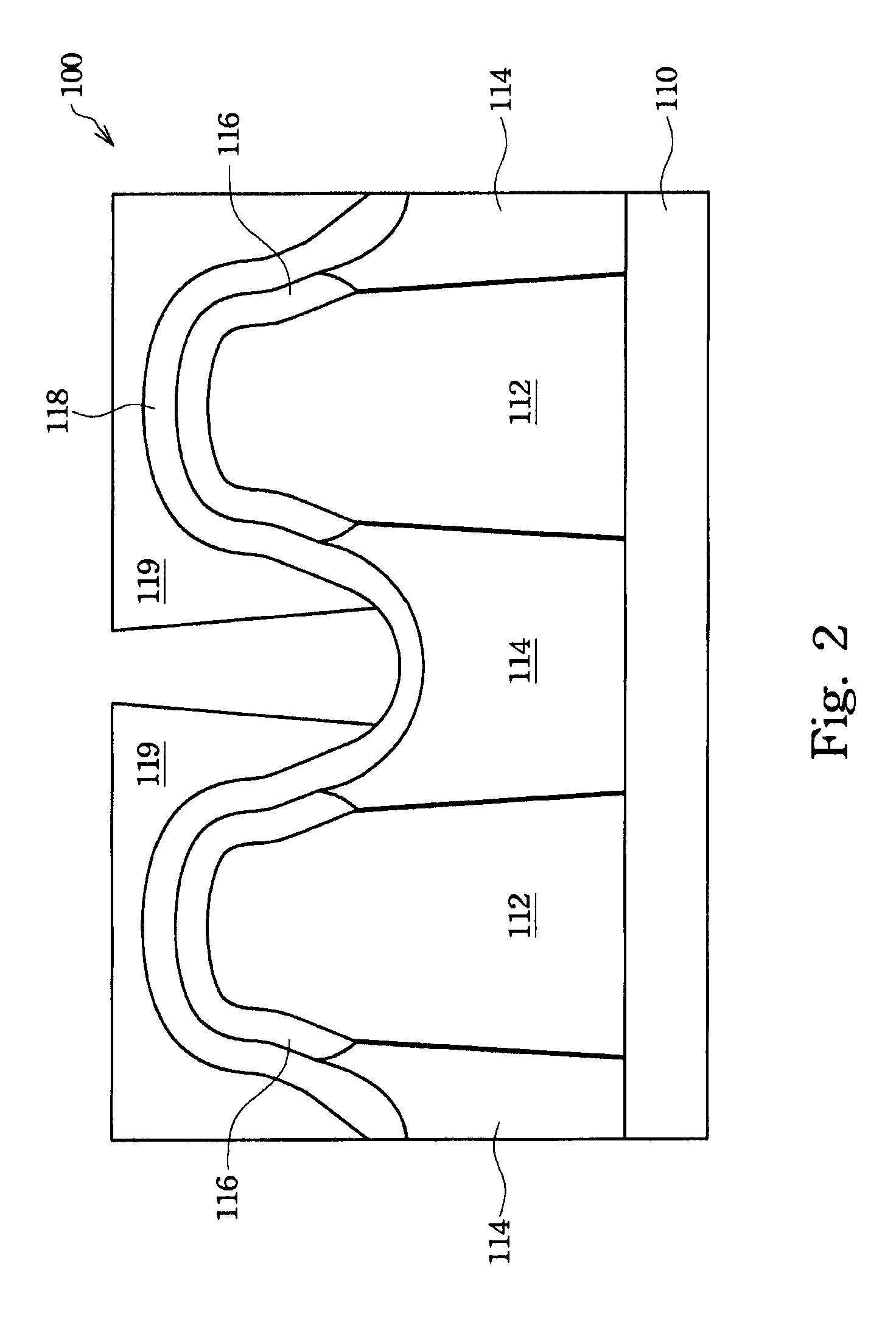
[0005]In non-volatile memory devices, NAND memory cells have various advantages including efficiency and reduced dimensions. Currently, a non-planar NAND memory architecture is utilized with a structure similar to FinFET transistors and with recessed shallow trench isolation (STI). However, the silicon nitride layer of the NAND memory cells for charge trap directly con...
PUM
| Property | Measurement | Unit |
|---|---|---|
| temperature | aaaaa | aaaaa |
| temperature | aaaaa | aaaaa |
| dielectric | aaaaa | aaaaa |
Abstract
Description
Claims
Application Information